This file type includes high resolution graphics and schematics when applicable.
Ultrawideband (UWB) communications systems promise impressive bandwidths at low power levels through the use of time-coded pulses spread over a wide spectrum. While building a receiver capable of covering wide bandwidths is a challenge, creating the impulse generator to go with such an architecture can also be difficult. Fortunately, it is possible to assemble a relatively simple, low-cost, low-power UWB impulse generator by using a step-recovery diode (SRD) and a resistive-capacitive (RC) high-pass filter. This impulse generator has been produced using microstrip circuit technology and yields impulses with full width at half maximum (FWHM) of less than 200 ps and at pulse repetition frequencies (PRFs) to 200 MHz.
Generation of subnanosecond impulses with an SRD is governed by the diode’s snap time (transit time) and junction capacitance; the PRF is dominated by the diode’s minority carrier lifetime. To generate ultrashort pulses, a SRD with short transit time and low junction capacitance is usually selected. This type of SRD is expensive and may limit the PRF. To improve the PRF by 10 to 20 times faster, a SRD with longer transit time and minority carrier lifetime should be used. Therefore, the design of an SDR-based impulse generator is a trade-off in performance to achieve either higher PRF or subnanosecond FWHM duration.
To minimize ringing in the impulse generator, pulse shaping is vital. Reported known techniques for accomplishing this include an approach that combines a MESFET amplifier and Schottky diode,1 the use of a resistive matching network and Schottky diodes for rectifying and switching,2,3 and simple impedance matching circuitry realized with microstrip line stubs.4
In the present design approach, rather than use an expensive SDR and a Schottky diode, a low-cost silicon SRD with long transit time was combined with a few lumped elements for impulse shaping (filtering) to generate ultrashort impulses with minimal ringing effects. This cost-effective approach may be as much as 100 times less expensive than the techniques detailed in references 1-3. The simplicity of this design approach also significantly reduces the overall printed-circuit-board (PCB) dimensions required as compared to the existing design techniques in references 1-3.
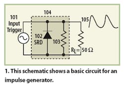
The fundamental elements required to generate impulses are a resistor and an SRD. An SRD placed in series to a microstrip line circuit can generate steplike pulses when it is excited by an input signal, which could be either sinusoidal waves or rectangular pulses. However, this circuit requires a quarter-wavelength short-circuited stub to generate impulses through reflections.2 To minimize the dimensions of the PCB used for the impulse generator, the SRD can be connected across microstrip lines in a shunt configuration so that the short-circuited stub is not needed. This simpler approach was used in the schematic circuit shown in Fig. 1, where the label 104 refers to the impulse circuit, label 102 to the SRD, and label 103 is a resistor placed in a shunt connection across the transmission line.
The SRD used in this report was a model MA44769 diode from M/A-COM (www.macom.com) with a cost of less than $0.65. It features a transition time of better than 150 ps, junction capacitance of about 1 pF, and moderate carrier lifetime of 30 to 50 ns.
When an input trigger signal (label 101 in the schematic diagram of Fig. 1) is fed to the impulse circuit, the SRD (label 102 in the circuit) is charged during the input signal’s positive cycle and discharged during the input signal’s negative cycle to form impulses. The resistor (label 103 in the schematic) provides a ground reference for the SRD. Since the SRD has a long transition time, the impulse generated at the output (label 105 in the schematic) has typical pulse width (FWHM) of 3 to 5 ns. By inverting the polarity of the SRD, the generated impulse will be 180 deg. out of phase.
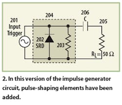
To shape these generated impulses into subnanosecond pulses, a capacitor (label 206 in the schematic of Fig. 2) is connected in series at the output of the impulse circuit (label 204 in the schematic of Fig. 2).
To limit the generation of low-frequency signal components, a capacitance in the range of a few picofarads is recommended for this capacitor.
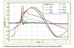
The circuitry for the low-cost impulse generator was realized on a PCB of RO4350 substrate material from Rogers Corp. (www.rogerscorporation.com). The material, with a dielectric constant of 3.48, was used in a thickness of 0.762 mm. For the input trigger (label 201 in the schematic of Fig. 2), a 100-MHz continuous-wave (CW) source was set at a power level of +10 dBm (2 V peak to peak). Depending on the value of capacitor 206, the impulses are shaped into different pulse durations at output 205, as shown in Fig. 3.
A resistor can be placed in series at the input of the impulse circuit (at 204) to prevent feedback signals from triggering the source. However, the loss from this resistor may require the use of a higher-amplitude input signal to excite impulse generation.
Inverting the polarity of the SRD may generate similar results as shown in Fig. 3 but the impulse formed would be inverted (180 deg. out of phase). To avoid confusion, all the measurements presented in this article refer to impulses with positive polarity and the anode of the SRD is connected to the ground.
To further improve the performance of the impulse circuit, a DC supply was added as shown in Fig. 4.
The resistor (shown as 103 in Fig. 1 and 203 in Fig. 2) has been repositioned as resistor 303 in Fig. 4. The placement of the resistor prevents leakage of high-frequency signal components to the DC bias network. In the modified circuit of Fig. 4, the capacitor (now labeled 306) remains as the impulse-shaping element as well as a DC blocking device.
The capacitor labeled 307 has been introduced at the input of the impulse circuit as a DC blocking capacitor while the capacitor labeled 308 behaves as an AC bypass device. These capacitors are selected in the range of a few hundred nanofarads. The biasing voltage to the impulse generator circuit, VDC, should be within the VThreshold range shown in Fig. 5.
This condition is only true if the SRD is shunted across the transmission line and its anode is connected to ground. The optimum and passive ranges shown in Fig. 5 will be swapped if the polarity of the SRD is inverted. As a result, the impulse generated at the output (305) will also be 180 deg. out of phase.
Page Title
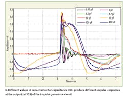
With different value of capacitance for capacitor 306, measurements (Fig. 6) revealed that the impulse becomes narrower with lower capacitance values.
By comparing the results shown in Figs. 3 and 6, it can be seen that higher amplitude is possible by optimizing the impulse circuit. The output of the impulse generator is a simple RC high-pass filter that is realized by capacitor 306 and the load impedance (which is 50 ohms in this case). The pulse width at FWHM, , can be roughly estimated by:
π= RC
π= 50 * C
where:
C = the capacitance of capacitor ‘306.’
In conclusion, it has been shown that the optimized impulse circuit is able to convert 100 MHz, +10-dBm CW signals into impulses with better than 180 ps FWHM, rise time of less than 120 ps (10 to 90 percent of the pulse amplitude), and peak-to-peak amplitude of greater than 850 mV, given a capacitor (306) with value of 2.2 pF. The operable PRF of the impulse generator ranges from 1 to 200 MHz, depending on the input excitation frequency and signal amplitude. The circuit is capable of generating impulses at PRFs as low as 100 kHz, although the amplitude will be somewhat low.
REFERENCES
- J.S. Lee and C. Nguyen, “Novel low-cost ultra-wideband, ultra-short-pulse transmitter with MESFET impulseshaping circuitry for reduced distortion and improved pulse repetition rate,” IEEE Microwave Wireless Component Letters, Vol. 11, May 2001, pp. 208–210.
- J.S. Lee, C. Nguyen, and T. Scullion, “New uniplanar subnanoseconds monocycle pulse generator and transformer for time-domain microwave applications,” IEEE Microwave Theory and Techniques, Vol. 49, No. 6, June 2001, pp. 1126-1129.
- J. Han and C. Nguyen, “A new ultra-wideband, ultrashort monocycle pulse generator with reduce ringing,” IEEE Microwave and Wireless Components Letters, Vol. 12, No. 6, June 2002, pp. 206-208.
- K. Madani, “A 20-GHz Microwave Sampler,” IEEE Microwave Theory and Techniques, Vol. 40, pp. 1960–1963, October 1992.
This file type includes high resolution graphics and schematics when applicable.


