Download this article in .PDF format
Transistor amplifier designers rely on numbers to match active devices to surrounding circuitry and to each other. They may select a transistor from a catalog, but the circuit designer has no influence over the transistor's parameters. These are set by the device's geometry, the quality of the manufacturing process, and semiconductor physics. As a result, the circuit designer must be guided by a device's measured scattering parameters (S-parameters) to determine the circuit-element values needed to surround an active device or devices in an amplifier design. This first installment of an eight-part design series will explore S-parameters; the series itself will transform any reader into a full-fledged amplifier designer.
To the circuit designer the transistor is a two-port network described by a table of S-parameters that have been measured over the frequency domain for which it has gain. After the bias and heat sinking needs of the transistor have been satisfied, the RF design proceeds using these S-parameters. At this point it is of no consequence whether the device is a bipolar transistor, a field-effect transistor (FET), or any other device whose S-parameters indicate the prospect of gain.
S-parameters are based upon the concept of incident (ai) and exiting (bi) waves. Customarily the bi waves are called reflected waves, but "exiting" is a better term since portions of the bi waves actually may result from energy that passes through rather than is reflected from the network. By using a and b waves, a linear network can be characterized by a set of simultaneous equations describing the exiting waves from each port in terms of the incident waves at all of the ports. The constants that characterize the network under these conditions are called S parameters.
For example, for a two-port network, the b wave leaving Port 1 (b1) is the phasor sum of a wave reflected from the input port (S11a1) plus a wave that passed through the two-port from Port 2 (S12a2). That is,
See associated figure
and
See associated figure
where:
See associated figure
See associated figure
and the voltage at port 1, for example, is the sum of an incident voltage and a reflected voltage (V1 = V1I +V1R). Similarly, the current at port 1 is the sum of an incident current and a reflected current (I1 = I1I +I1R). The normalized incident (ai) and reflected (bi) waves can be measured with the aid of directional couplers with matched source and loads presented to the two-port terminals. This is equivalent to the measurement provided by a network analyzer. This measurement simplicity underlies the advantage of the S parameters, but it introduces a complication. Whereas the alternate Z, Y, and ABCD parameters depend only upon the network being measured, the S-parameter values depend both upon the network and the characteristic impedances of the source and load used to measure it. More about the consequences of this condition will be presented later in this article series.
When the source and load impedances are the same as those used to determine the S-parameters, the magnitude of S21 is the ratio of the outgoing wave, b2, to the incoming wave, a1. Hence, it is equivalent to the voltage or current gain of the amplifier. Similarly, the magnitude of the square of S21 is equal to the power gain.
As an example, suppose we wish to design an amplifier to operate at 1 GHz with 50- source and load impedances. On reviewing tables of S-parameters provided in a catalog or in an electronic file within a circuit simulator, suppose that the Motorola 2N6679A bipolar transistor is selected for the amplifier design. The table shows its S-parameters in standard format.
The magnitude of S21 can be seen as 6.6 at 1 GHz. The basic gain, without tuning, in a 50- system is:
See associated figure
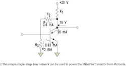
At this point, if this is considered satisfactory gain, it is simply a matter of designing a bias circuit.2 For bias, a 20-V source should be used, since the S-parameter file indicates the performance was obtained with a 15-V bias between collector and emitter. From the transistor data, it can be seen that the performance was obtained with VCE = 15 V and IC = 25 mA. The DC current gain, = IC/IB, is not listed in the S-parameter file, but on contacting the manufacturer, suppose that at room temperature = 40. Based on this information, the biasing network of Fig. 2 was developed.
The resistor values are calculated as follows. A base current of 0.63 mA is required (25 mA/40). However, a shunt path to carry about five times this value, say 3 mA, is desirable so that when the 15-V level falls, the base current will fall nearly proportionately. Since the transistor is a silicon NPN, the base-emitter junction behaves as a silicon diode. Hence, it will have a voltage drop at turn-on of about 0.75 V. The emitter-base shunting resistor can be calculated as:
See associated figure
See associated figure
See associated figure
Practically speaking, the closest values of standard resistors may be used. This bias circuit tends to self-compensate with temperature. As temperature increases, the base current increases for a given VBE. However, this causes an increase in IC, resulting in a larger voltage drop in R1, and thereby reducing VBE.
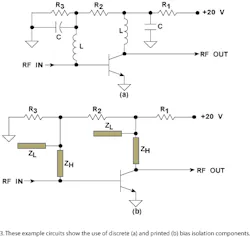
By themselves, resistors R2 and R3 are large compared to the 50- RF impedance level at the input. However, their parasitic elements may cause them to place an excessive load on the RF circuit. Furthermore, it is undesirable to have RF signals present in the bias circuit, since this may cause undesired RF radiation. Therefore, circuitry to isolate the bias from the RF signals is employed (Fig. 3).
Basically, the bias isolation circuitry presents a high RF impedance from the transistor terminals to those of the bias circuitry. This can be accomplished using discrete components (Fig. 3a). For the present 1 GHz, 50- amplifier example isolating elements of L=100 nH and C = 100 pF might be employed. When space permits the isolating elements can be "printed" as distributed elements along with the RF circuit. The transmission lines are one-quarter wavelength long at the amplifier's RF center frequency. For the 50- amplifier example, the high-impedance lines might be made ZH = 150, and the low-impedance lines ZL = 25-.
Bias isolating networks are crucially important in amplifier design and should not be taken for granted in the design effort. As shall later be seen, transistors may have gain at frequencies well above the design bandwidth. In the present 1-GHz amplifier example, the table shows that the transistor has gain above 5 GHz. It also has the potential of breaking into oscillation at any frequency for which it has gain (this potential instability will be addressed in the next installment of this article series).
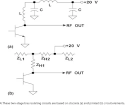
The single-stage bias circuits shown in Fig. 2 have only single high-impedance and low-impedance elements for isolation. They are shown for illustration of the bias isolating methods and are not presented as adequate designs for all applications. Where practical, multistage bias isolation is preferable (Fig. 4).
An informal measure of the effectiveness of the distributed bias structure is to bring a screwdriver tip near the open circuit ends of the bias flags (the open-circuited ends of the low impedance line sections) while measuring the output power of the amplifier. A significant power change experienced when so probing the end of the second bias flag, ZL2, indicates the bias circuit may be resonant at the wrong frequency or that more isolating stages are required.
Most commercial computer-aided-engineering (CAE) circuit simulators can work with an S-parameter table to provide an analysis over frequency, interpolating the data to calculate the circuit behavior between frequencies for which actual measured S-parameter data are available. The circuit evaluation could be performed with bias elements but it is assumed in this article that sufficient bias isolation is achieved that only the RF circuit need be considered. The gain of the present example, using the 2N6679A transistor, was simulated in Fig. 5 using the Genesys CAE simulation suite from Eagleware Corp. (Norcross, GA). The impedance of the input and output ports is 50 unless otherwise noted.
At this point, if this gain is satisfactory (and overlooking for the present time the matter of amplifier stability), the electrical portion of the amplifier design is complete. On the other hand, on examining the input and output reflection coefficients, S11 and S22, respectively, in the table, it is apparent that a good amount of power is lost to reflection at the input and mismatch at the output. At 1 GHz,
See associated figure
These mismatch losses correspond to 46-percent power loss at the input and 21-percent power loss at the output. Therefore, by matching input and output, as much as 3.7 dB additional gain can be added, with a matched circuit at input and output as well. Next month, Part 2 of this article series will examine the means of matching the transistor to obtain this additional gain and present what is necessary to guarantee unconditional stability.
EDITOR'S NOTE
This article is excerpted with permission from the one-week industrial couse, Wireless Engineering, that the author teaches and from High Frequency Techniques, An Introduction to RF and Microwave Engineering; by Joseph F. White (John Wiley & Sons, Hoboken, NJ, 2004; e-mail: www.Wiley.com).
| REFERENCES | 1.Genesys 7 Reference Manual, (Eagleware, Norcross, GA, 1986-2000). 2. Guillermo Gonzalez, Microwave Transistor Amplifiers, Analysis and Design, 2nd ed. (Prentice-Hall, Upper Saddle River, NJ, 1984), pp. 273-283. |


