Ensure Stability In Amplifier Designs
Download this article in .PDF format
Amplifiers can be designed as simply as by installing a transistor in a 50-Ω system. As was shown last month in the first installment of this article series, in this simple case, the gain at each frequency was just the square of the magnitude of S21 as listed in the S parameter table for the transistor. Additional gain could be obtained at any given frequency for which the transistor has gain by adding matching circuits at the input and/or at the output. This second part of the article series will examine the stability of a transistor amplifier and how to apply stabilizing elements to obtain it.
Thus far, the transistor has been treated as a unilateral device, with signals assumed to pass from the input to the output but not in the reverse direction. Making the unilateral assumption is equivalent to assuming that S12 is zero. The S12 parameter provides the feedback term by which power from the output circuit (which may be relatively high due to the transistor's amplification) can feed back to the input. When it does so, it may combine with reflections already present at the input to produce an effective S11 whose magnitude exceeds unity. This corresponds to reflection gain, and a transistor amplifier that can experience this gain, is termed conditionally unstable, the conditions being certain combination(s) of load impedance, S12 and S11 to produce self-oscillation (instability).
In the 2N6679A transistor amplifier example, the magnitudes of S11 and S22 of the transistor are less than one for all frequencies. This means that the transistor is stable when embedded between 50-Ω source and load, and it will not oscillate. However, this is not considered unconditional stability, because with different source and load impedances the amplifier might break into oscillation. A properly designed (stabilized) amplifier will not oscillate no matter what passive source and load impedances are presented to it, including short or open circuits of any phase.
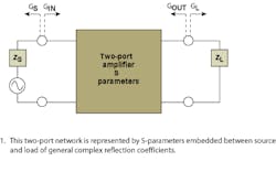
Because the value of S12 for practical transistors is not zero, a signal path exists from the output (where power levels are higher due to the device's gain) to the input (Fig. 1).

It is possible that for certain values of load reflection coefficient, ΓL, the input reflection coefficient, ΓIN, can exceed unity, turning the circuit into a reflection amplifier at the input. Similarly, certain values of source reflection coefficient, ΓS, at the input might cause the output reflection coefficient, ΓOUT, to exceed unity magnitude. If either or both of these conditions can occur at any frequency, the circuit is said to be only conditionally stable, or equivalently, potentially unstable.
The boundary line between stable and unstable operation at the input is the |ΓIN| = 1 circle centered at the origin of the Smith Chart. The contour of values for ΓL (also a circle) that produces a unity magnitude reflection coefficient at the input is called the input stability circle (shown in Fig. 2 at 1 GHz for the 2N6679A transistor).
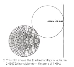
The input stability circle represents a set of load reflection coefficients that cause the input reflection coefficient to have a unity magnitude. Also note that the input stability circle represents a boundary, on one side of which |ΓIN| IN| > 1, corresponding to load impedances that produce potential instability.
The ΓL values are related to the ΓIN values according to Eq. 1, which is called a mapping function because it maps a IN contour into a ΓL contour (pp. 140-145 in ref. 1). This function maps the |ΓIN| = 1 function into a ΓL contour (in this case, a circle) to a circle:
Inserting the condition |ΓIN| = 1 into Eq. 1 creates a mapping of the |ΓIN| = 1 circle into the input stability circle in the ΓL plane with center at the
and a radius of
The input stability circle is also called the load instability circle, because it describes the ΓL values that border on causing instability, that is which result in |ΓIN| = 1. The input stability circle will be referred to as the load instability circle because this nomenclature places the focus on the load impedances that cause instability.
The circle intersects and intrudes into the unity radius area of the Smith Chart. Thus, the transistor is potentially unstable for certain passive load impedances bounded by the circle. The circle is the boundary of the unstable impedances. Since it is only the boundary, when the circle is first plotted, it is not certain whether the unstable load impedances are those inside or outside the circle. In the example of Fig. 2, it would seem highly likely that the unstable points are inside the circle, since most of the circle is in the negative resistance domain of the Smith Chart. However, there are instances in which the entire circle may lie within the unity-radius, passive-impedance portion of the Smith Chart. A means for determining which side of the boundary represents the unstable impedances is needed. The determination is facilitated by the availability of the S-parameters, which apply with a known load, usually 50-Ω.
To determine whether the unstable load impedances are inside or outside the circle, consider the "easy point," S11. From the S-parameter file for the 2N5579A transistor, it is known that when the transistor is loaded with 50-Ω, the center of the Smith Chart, |S11|
Figure 2 also shows that high inductive load impedances at the output can cause instability (at the input). The points outside the Γ = 1 circle correspond to loads with negative resistance. These are of no concern, because any amplifier might be made unstable by subjecting it to a given source or load impedance with a negative real part. Amplifier stability only requires that the circuit be stable with passive input and output reflection coefficients, that is, passive source and load impedances.
Next, consider the source reflection coefficients that cause |ΓOUT| = 1. The relation of ΓS to ΓOUT is given by (see p. 142 of ref. 1):
In a similar fashion, this can be used to map the |ΓOUT| = 1 circle onto the ΓS plane:
and radius of
Plotting this for the transistor at 1 GHz gives the left circle outside the Smith Chart in Fig. 3.
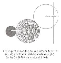
The output stability circle is also called the source instability circle because it represents those ΓS values that cause instability in the input circuit. The points within the output stability circle are unstable ones because, from the S-parameters of the transistor, |S22| OUT| > 1) at low input source impedances.
These circles indicate certain characteristics of the transistor. For example, any attempts to obtain more gain from the transistor by adding matching circuits at the input and output must avoid those impedances that would cause instability. Even if the transistor is used with only 50-Ω loads, if the source or load is removed and there is a transmission line whose length transforms an open circuit to one of the unstable impedances, the circuit may oscillate.
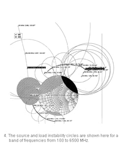
The examples so far have only examined the transistor's behavior at 1 GHz. For an amplifier to be unconditionally stable, however, it must be stable at all frequencies (at which the device has more than unity gain). The resulting source and load instability circles are two separate families of circles(Fig. 4).
Since the stability circles can be calculated directly from the S-parameters, it would seem that stability could be determined from the S-parameters themselves, without need for the stability circles. To do this, first define a stability factor, K, as (see p. 145 of ref. 1)
where:
The amplifier is unconditionally stable provided that
and
Equivalently (see p. 324 of ref. 2), the amplifier is unconditionally stable if
and
where:
Applying this test to the 2N6679A transistor and using the Genesys computer-aided-engineering (CAE) program from Eagleware (Norcross, GA) to calculate K and B1 gives the results in Table 1. From these values, it is apparent that the transistor is potentially unstable at 1 GHz (and other frequencies), as had already been deduced from the input and output stability circles. The source instability circles indicate that low impedances at the input may cause instability. This suggests that a resistance placed in series with the base lead can reduce the intersection of the source instability circles with the |Γ| 1 circle, which will also reduce gain. However, since device instability usually peaks at low frequencies (at which the transistor has the highest gain), the resistor can be shunted with a capacitor to reduce its effect near 1 GHz. One such stabilizing circuit is shown in Fig. 5.
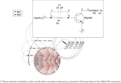
This measure almost removed all instabilities. It moved both the source and load instability circles away from the |Γ| = 1 (passive Smith Chart) portion of the reflection coefficient plane(Fig. 6).
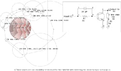
Rather than add more resistance to the base lead, it is often found to be more effective to add some damping to the output. Corrections to the input stability tend to help the output stability, and vice versa.
Examining the load instability circles reveals that high output load impedances cause instability. To counter this, shunt resistance can be added at the output, placed at the end of a high-impedance 90-deg. line at 1 GHz to minimize its effect at that frequency. The shunt resistance limits how large the load impedance can be, minimizing the likelihood that a high impedance that can cause instability will be encountered at the output.
This addition to the output circuit has unconditionally stabilized the device over the 100-to-2000-MHz range, in which it previously was potentially unstable. From the K factor calculations (Table 2) it can be seen that the low-frequency range is well stabilized. This is important because S-parameter data below 100 MHz were not included in the S-parameter file.
The resulting gain of the 2N6679A with the stabilizing elements is shown in Fig. 7.
In comparing this gain with that of the unstabilized transistor of Part 1, only about 0.6 dB gain is lost at 1 GHz, dropping from 16.4 dB to about 15.8 dB. The low-frequency gain has been reduced even more, which is actually a benefit. Gain outside the desired bandwidth is a liability, because it can cause instabilities. Next month, readers will learn how to match an amplifier's input and output ports for additional gain using the unilateral gain method.
EDITOR'S NOTE
This article is excerpted with permission from the one-week industrial course, Wireless Engineering, that the author teaches and from High Frequency Techniques, An Introduction to RF and Microwave Engineering, by Joseph F. White (John Wiley & Sons, Hoboken, NJ, 2004; www.wiley.com).
