LNA Integrates Fast Shutdown Function
This file type includes high resolution graphics and schematics when applicable.
Time can be critical in modern communications systems, such as time-division-duplex (TDD) wireless systems. Although frequency-division-duplex (FDD) approaches have long dominated cellular communications systems, limited spectrum and high cost are making TDD approaches more attractive, as evidenced by growing use of standards such as time-division synchronous code-division-multiple-access (TD-CDMA) and TD Long Term Evolution (LTE) standards.1,2 To prevent dead time in TDD switching, reception should ideally commence as soon as transmission has ended.
However, a cellular system’s low-noise amplifier (LNA), which is typically shut down during transmission to prevent damage of active devices and receiver overload, can suffer delays in returning to its active state. Because of these delays, a “guard time” of about 2% of the channel time must be allocated as settling time for the wireless system’s hardware.3 When transmission recommences, any delay in shutting down the LNA can result in temporary receiver overload.
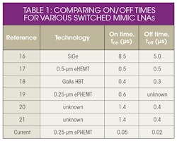
In older wireless system implementations, the shutdown function was external to the LNA device. To reduce parts count and enable miniaturization of the LNA, the amplifier and its shutdown function are now typically integrated in a monolithic microwave integrated circuit (MMIC). Such MMICs are commercially available with switching speeds ranging from one-half microsecond to several microseconds (Table 1).
To enable further reduction in TDD dead time, a MMIC LNA was developed with an on-chip switching circuit optimized for speed. In addition to providing the fastest switching speed in this device class, this new LNA design must also meet the stringent noise and linearity requirements demanded by the cellular infrastructure. This article discusses the design considerations and then reports the performances achieved.
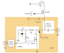
Diode resistance RD limits the current through diode D. The forward-biased diode generates wideband noise and capacitance C is required to suppress that noise. Unfortunately, this capacitance requires a finite amount of time to charge and discharge. The time constant associated with RDC slows the rise time of the gate voltage VGSat with power on, while RGC delays gate bias VGS from decaying to zero at shutdown.
Additionally, the combination of the supply bypass capacitor Cbypass and the switching transistor’s “on” resistance (typically 25 to 200 Ω4) can also slow down the switching speed, particularly if a large value of Cbypass is chosen to effectively suppress supply transients. Because of these unavoidable time constants, an externally switched MMIC LNA will be limited in switching speed. Typical switching speeds range from about 1 to 4 μs (Fig. 1).5
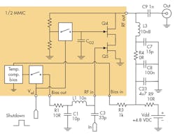
The MMIC is fabricated by means of a proprietary 0.25-μm enhancement-mode pseudomorphic high-electron-mobility-transistor (ePHEMT) process on 6-in. wafers.6,7 The MMIC integrates dual amplifiers, adjustable active biasing, and shutdown functions housed in a 16-pin 4 × 4 × 0.85 mm quad-flat-no-lead (QFN) package.8,9 A cascade configuration (Q4-5) was chosen for the amplifier because one common-source stage cannot meet the target gain at S-band (Fig. 1).
The cascade configuration’s bottom gate is biased by a temperature-compensated voltage reference and the top gate is biased by a resistor divider. During shutdown, both gates are disconnected from their respective biasing sources by internal transistor switches. Because gate current is in the microampere range, small switching transistors can be used for this purpose. This minimizes the speed-robbing junction capacitance and helps maintain small overall chip area. Although interrupting either one of the two gate supplies is sufficient to shut down the cascade amplifier configuration, switching both gates simultaneously improves the forward isolation and the switching speed of the LNA switch function.
Because the switches are fabricated on the same high-speed process as the RF amplifier [with transition frequency (fT) of about 55 GHz], their propagation delays are small in comparison to the overall switching time. On the other hand, the RC components, required to bias and decouple the cascode gates, can slow down the switching speed through their time constants. Since the biasing components are necessary, the only way to mitigate their effect on the switching speed is to choose the smallest usable values for capacitances C1 and CG2 and the connected resistances.
In contrast to the externally switched example (Fig. 1), the monolithic integrated shutdown function permits large-value capacitances to be used for bypassing the supply (e.g., C8 and C23) without sacrificing switching speed; larger value capacitances confer greater immunity to supply transients.10 The cascode’s input and output impedances are matched by L1 and C3 and L3 and C9, respectively. These components form highpass LC networks and are dimensioned for operation at 2.6 GHz, i.e., the UMTS VII band.11 The supply voltage Vdd is +4.8 VDC and the current is about 55 mA.
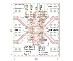
The prototype LNA was assembled on 10-mil-thick Rogers RO4350B printed-circuit-board (PCB) material from Rogers Corp., where 50-Ω microstrip traces are 0.58 mm wide (Fig. 3). The RO4350B material has a dielectric constant of typically 3.48 in the z-direction (through the thickness) at 10 GHz. An FR-4 backing layer provides rigidity and increases the stack height to 1.6 mm to suit edge-launch SMA receptacles.
This file type includes high resolution graphics and schematics when applicable.
Making Measurements
This file type includes high resolution graphics and schematics when applicable.
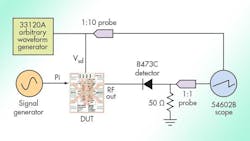
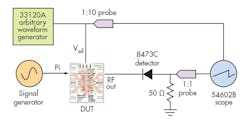
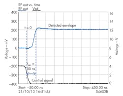
The time taken to switch from one LNA state to another has been variously referred to as “switching time/speed/rate” and “power settling time” due to absence of a standardized terminology. The turn-on time, tON, is measured from 50% of the control signal to 90% of the final output amplitude.12,13 The turn-off time, tOFF, is similarly defined. The setup (Fig. 4) for evaluating the LNA switching speed follows.13 An RF signal generator feeds the LNA with a 2.6 GHz, 0-dBm carrier.
A pulse generator [alternatively, a function generator or an arbitrary waveform generator (AWG)] provides the logic-level control signal for the switches. The envelope of the amplified carrier is detected by a low-barrier Schottky diode detector. The output of the Schottky detector is loaded with a 50-Ω feedthrough resistor to quicken its response time to between 8 and 12 ns.14
As part of the switched-LNA test setup, an oscilloscope displays the detected envelope and the control signal; the rising/falling edge of the control signal triggers the oscilloscope. Although a spectrum analyzer can replace the combination of a diode detector and an oscilloscope, the latter was selected for its fast response time compared to the slow response time of a spectrum analyzer, which can artificially inflate any measurements of LNA switching time.15
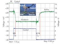
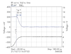
To shut down the LNA, the control logic voltage, Vsd, changes level from “LOW” to “HIGH” (Fig. 6). Correspondingly, the detected envelope, RFout, decreases from about 200 mV to 0 V. Referenced to the control-signal midpoint, the detected envelope (RFout) requires 0.02 μs to drop to 10% of its maximum value.
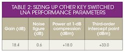
The actual tOFF time is most likely faster than the experimental value of 0.02 μs because it is very close to the diode detector’s specified response time (≤0.012 μs). In addition to its outstanding switching speed, the prototype switched LNA exhibited excellent performance levels in various other parameters, as detailed in Table 2.
In conclusion, this integration of the shutdown function with the LNA circuitry not only provides benefits in terms of the LNA parts count and size, but also avoids the high current levels and slower speeds associated with external switching solutions. A combination of fast pHEMT technology, dual switches, and optimum circuit connections enable this design to be more than one order magnitude faster than its closest competitor. This switched LNA offers the potential to significantly trim the “guard time” required by LNAs in TDD wireless communications systems.
Acknowledgments
The author would like to thank H.A. Zulfa and Y.H. Chow for the IC design; S. Punithevati and M.D. Suhaiza for assembling the prototypes; and S.A. Asrul and the management of Avago Technologies for approving the publication of this work.
References
1. Lou Frenzel, “What’s the difference between FDD and TDD?” Electronic Design (online), July 2012.
2. B. Li, D. Xie, J. Chen, P. Zhang, and W. Zhu, “Recent advances on TD-SCDMA in China,” IEEE Communications Magazine, January 2003, pp. 30-37.
3. D. Barr, S. Shellhammer, R. Jain, and J. Montojo, “Introduction to TDD,” presented at the IEEE EPoC PHY Study Group Meeting, May 15-16, 20XX, Minneapolis, MN.
4. P. Horowitz and W. Hill, “Limitation of FET Switches,” Chapter 3.12 in The Art of Electronics, Wiley, Cambridge, England, 1997.
5. G. Watkins and S. Wang, “The impact of power amplifier turn-on characteristics in cognitive radio networks,” Microwave Journal, March 2014, pp. 86-92.
6. D.W. Wu, J.S. Wei, C. Su, R.M. Parkhurst, S.L. Fu, S. Chang, and R.B. Levitsky, “An enhancement-mode PHEMT for single-supply power amplifiers,” Hewlett-Packard Co., Palo Alto, CA, Hewlett-Packard Journal, February 1998.
7. K. Fujii and H. Morkner, “Single supply 1W Ku-band power amplifier based on 0.25-μm E-mode PHEMT,” Microwave Symposium Digest, 2006.
8. Avago Technologies, datasheet, “MGA-16316 dual LNA for balanced application 1950-4000 MHz,” October 2012.
9. C.L. Lim, “Compact LNA Drives 2.5-GHz Base Stations,” Microwaves & RF, January 2014.
10. Hewlett-Packard Co., Application Note A001, “Notes on choke network design,” 1993.
11. Wikipedia, “UMTS frequency bands."
12. V.K. Varadan, K.J. Vinoy, and K.A Jose, “RF MEM switches and micro relays,” in RF MEMS and Their Applications, Wiley, London, 2003, Chapter 3, p. 112.
13. Agilent Technologies, Application Note, “Understanding RF/microwave solid state switches and their applications,” May 2010.
14. Agilent Technologies, datasheet 5952-8299, “423B, 8470B, 8472B, 8473B/C low barrier Schottky diode detectors,” October 2011.
15. A. H. Abdelmajid, “Accurate measurement of On/Off time for 802.11 b/g WLAN/WiMAX LNAs,” High Frequency Electronics, November 2009, pp. 18-25.
16. Maxim Integrated Circuits, Application Note 1191, “The MAX2644 meets 10 μs switching time for 802.11b WLAN LNA,” September 2002.
17. Avago Technologies, Application Note 5387, “MGA-675T6.”
18. D. Zhao, “RF2374 meets switching time for WLAN/WiMAX LNA,” October 2008.
19. C.L. Lim, “LNA lowers noise, raises OIP3 at 3.5 GHz, Microwaves & RF, July 2011.
20. NXP Semiconductors, datasheet for BGU8051, revision 2, December 2013.
21. NXP Semiconductors, datasheet for BGU8053, revision 2, December 2013.
This file type includes high resolution graphics and schematics when applicable.
