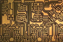
PCBs At Microwave Frequencies: Design Guidelines
This file type includes high resolution graphics and schematics when applicable.
Laminate printed-circuit boards (PCBs) are a commonly used substrate for designing low-cost subsystems that can operate to 40 GHz. With their ability to support high-performance surface-mount technology packages (SMTs) containing RF integrated circuits (ICs) while supporting a wide range of interface connections, PCBs are ideal for many RF/microwave applications. However, significant considerations must be applied to every step of the design to ensure proper operation. Such considerations have grown due to the reduction in size of RF ICs, which has led to a reduction in parasitic capacitance and a subsequent increase in attainable frequencies of operation. In a seven-page application note titled “Technology Overview‑Designing Laminate PCBs at Microwave Frequencies,” Plextek discusses some of these critical design considerations.
If appropriate measures are not taken, for example, grounding inductances can induce a series inductive feedback around an RF SMT IC. Two possible approaches to help reduce grounding inductances are the use of an array of tightly spaced vias within the groundplane of the SMT IC and selecting a suitably thin substrate height to reduce the individual via inductances. Knowing the level of tolerable grounding inductance and how to estimate the grounding inductance are necessary metrics to design with cost efficiency and timeliness.
The exact material and sizes of the PCB substrate also are critical for effective RF PCB design. Modern RF PCB substrates are well suited to mass manufacture and generally have dielectric constants around 3.5. To ensure appropriate operation of on-PCB transmission lines or microstrip waveguides, the maximum substrate thickness should be less than one-tenth of the highest wavelength of operation.
The thickness of the copper metallization, known as weights of copper cladding, must be known to design according to the required direct-current (DC) carrying capability as well as the maximum skin depth. The exact dimensions of the pads and metallization of attached discrete components and printed components correlate directly to the parasitic elements within the circuitry. They must therefore be accounted for accordingly. Based on the frequencies of operation, connections made with external devices (which usually incorporate on-board coaxial connections) and adequate grounding and mechanic attachment strength also should be taken into consideration.
Plextek Consulting, London Rd., Great Chesterford, Essex CB10 1NY, United Kingdom; +44 1799 533200.
This file type includes high resolution graphics and schematics when applicable.
About the Author
Jean-Jacques DeLisle
Jean-Jacques graduated from the Rochester Institute of Technology, where he completed his Master of Science in Electrical Engineering. In his studies, Jean-Jacques focused on Control Systems Design, Mixed-Signal IC Design, and RF Design. His research focus was in smart-sensor platform design for RF connector applications for the telecommunications industry. During his research, Jean-Jacques developed a passion for the field of RF/microwaves and expanded his knowledge by doing R&D for the telecommunications industry.

