Cascadable Gain Blocks Support Sub-10-GHz Designs

This article appeared in Electronic Design and has been published here with permission.
Components that support the last stage of the transmit-side RF signal chain and the first stage of receive-side complement—namely, the power amplifier (PA) and low-noise amplifier (LNA), respectively—get lots of attention for many reasons. However, internal intermediate gain stages in the signal chain also require their perhaps less-acknowledged components.
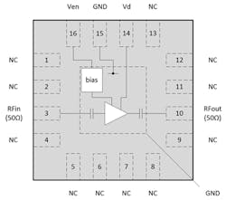
Addressing this gap, the CMX90G301 and CMX90G302 positive gain-slope amplifiers from CML Microcircuits are general-purpose gain blocks (Fig. 1). They’re well-suited to a wide range of wireless applications operating in the 1.4- to 7.1-GHz frequency range, including 4G/5G infrastructure applications and devices operating in license-free bands.
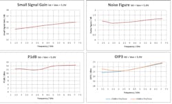
The CMX90G301 has +1-dB positive-gain slope, while the very similar CMX90G302 offers a +2-dB gain slope for applications requiring more gain-slope compensation. Both devices deliver a small-signal gain of 14.8 to 16.0 dB, a P1dB output rating of +11.5 dBm at 3.5 GHz, and a low noise figure of 2 dB. GaAs pHEMT technology is used to achieve an optimal combination of low dc power, low noise, and high gain.
Among the many graphs on the datasheet are those for basic performance of key parameters of small-signal gain, noise figure, P1dB output, and OIP3 (Fig. 2).
The CMX90G301 and CMX90G302 gain blocks are designed for ease of use, with a high level of integration and minimal need for supporting component, resulting in reduced PCB footprint as seen in the application schematic (Fig. 3). They eliminate the need for passive equalization circuits within the system design.
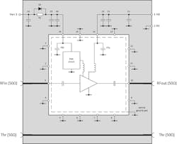
Further, due to their on-board active-bias circuit, the devices operate over a wide supply voltage of 2.7 to 5 V with a typical current of 22 mA. On top of that, the RF ports of each device are matched to 50 Ω, supporting rapid product development cycles, particularly for mass-market applications.
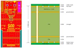
The datasheet also defines details of the 20- × 45-mm EV90G301 evaluation board, inducing the short bill of materials, top layer of PCB (Fig. 4), and even a cross section calling out the critical aspects of the layer stack of the PCB.
Both parts are housed in 3- × 3-mm VQFN-16 packages.
About the Author

Bill Schweber
Contributing Editor
Bill Schweber is an electronics engineer who has written three textbooks on electronic communications systems, as well as hundreds of technical articles, opinion columns, and product features. In past roles, he worked as a technical website manager for multiple topic-specific sites for EE Times, as well as both the Executive Editor and Analog Editor at EDN.
At Analog Devices Inc., Bill was in marketing communications (public relations). As a result, he has been on both sides of the technical PR function, presenting company products, stories, and messages to the media and also as the recipient of these.
Prior to the MarCom role at Analog, Bill was associate editor of their respected technical journal and worked in their product marketing and applications engineering groups. Before those roles, he was at Instron Corp., doing hands-on analog- and power-circuit design and systems integration for materials-testing machine controls.
Bill has an MSEE (Univ. of Mass) and BSEE (Columbia Univ.), is a Registered Professional Engineer, and holds an Advanced Class amateur radio license. He has also planned, written, and presented online courses on a variety of engineering topics, including MOSFET basics, ADC selection, and driving LEDs.
