Gigahertz Phased-Array Antenna Fabricated as Large-Area Sheet
What you’ll learn:
- How large-area electronics can be adapted to create a gigahertz phased-array antenna.
- The potential advantages of this approach versus discrete components.
- The test arrangement used and some test results on a three-element phased-array antenna.
Phased-array antennas are taking on increasing roles in MIMO systems such as 5G, as they can provide needed dynamic, all-electronic antenna steering and directivity. However, they have an attribute that complicates their physical and electrical fabrication—they’re composed of multiple identical, discrete antennas elements with form factors that aren’t amenable to mass-production techniques.
Responding to this dilemma, a team based at Princeton University devised and tested a technique for creating electronically steerable, GHz-range phased-array antenna assemblies as large-area electronics (LAE). They applied fabrication processes used for electronic circuits on thin, flexible materials.
The team adapted the scaling and electronic properties of LAE thin-film technologies and incorporated inductor-capacitor oscillators operating at gigahertz frequencies along with high-speed, self-aligned zinc-oxide thin-film transistors (TFTs). The oscillator circuits incorporate the frequency locking and phase tuning that are required for electromagnetic phased arrays (Fig. 1).
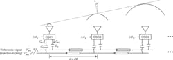
1. Architecture of the designed phased-array system consisting of a linear array of antennas at λ/2 spacing: Each antenna is driven by a localized oscillator (OSCi) that generates a sinusoidal voltage signal as excitation. A differential reference signal is coupled to each oscillator through a 50-Ω transmission line for injection locking. The phase of each oscillator is independently tuned, relative to the reference signal.
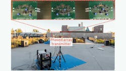
The researchers created a 30-cm linear array of three connected and controllable antennas (Fig. 2). The transistors and other components were fabricated on a glass substrate, but they said that a similar process could be used to create circuits on flexible plastic and thus enable it to conform to irregular or curved surfaces.
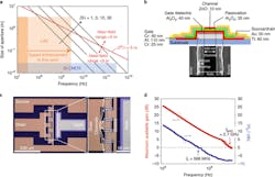
2. Values of D/λ of LAE and device optimization: (a) Comparison of aperture sizes and frequencies achievable by LAE and Si-CMOS technologies. (b) Schematic of the cross-section of a bottom-gate LAE ZnO TFT, and corresponding top-view SEM image highlighting the channel region self-aligned to the underlying gate. (c) Microscopy images of a ZnO TFT fabricated on glass. The TFT has six identical fingers, each of which is 25.0 µm wide and 0.7 µm long. (Inset: zoomed-in image of the channel region). (d) MAG and |H21| values of self-aligned ZnO TFT versus frequency. Frequencies at 0-dB crossings show the fMAX and fT values.
As noted by lead study author Can Wu, a postdoctoral researcher at Stanford University who completed a Ph.D. in electrical and computer engineering at Princeton earlier this year, “Large-area electronics is a thin-film technology, so we can build circuits on a flexible substrate over a span of meters, and we can monolithically integrate all the components into a sheet that has the form factor of a piece of paper,” earlier this year.
“People have tried discrete integration of hundreds of little microchips. But that's not practical—it’s not low-cost, it's not reliable, it's not scalable on a wireless systems level," added senior study author Naveen Verma, a professor of electrical and computer engineering and director of Princeton's Keller Center for Innovation in Engineering Education.
Testing the System
The system test setup consists of the phase-tunable oscillators that form the phased array, an arbitrary function generator (AFG), a vector-network analyzer (VNA), low-dropout voltage regulators (LDOs), and a receiver antenna followed by a low-noise amplifier (Fig. 3). The tests are controlled by a PC that starts the two-port scattering measurement in the VNA, which immediately triggers the AFG to generate an 85 μs-wide pulse. This enables the voltage regulators that provide the bias voltage to the capacitor banks.
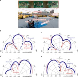
3. System demonstration: (a) Photograph of the test setup; the inset shows the three-element phased array. The phased array was mounted on a rotating rigid base. The reference (injection-locking) signal was provided by the VNA (all the cables were coated with EMI-shielding materials to avoid near-field interference). The receiver antenna was placed 3.4 meters away in the far field; its output was followed by a low-noise amplifier with its output fed back to the VNA and the magnitude of the radiated signal from the phased array was measured. (b, c, d, and e, respectively) Measured and simulated far-field radiation pattern at f0 = 982 MHz when the beam was steered to θ = 0°; at f0 = 982 MHz when the beam was steered to θ = 15°; at f0 = 982 MHz when the beam was steered to θ = –30°; and at f0 = 982 MHz when the beam was steered to θ = 30°. In the simulated pattern, the phase and magnitude variations are accounted for, and ideal omnidirectional antennas are assumed.
Next, 10 μs later, the AFG allows the voltage regulators that power up the oscillators for 65 μs to generate an electromagnetic pulse. The oscillators are frequency-synchronized and phase-tuned with reference to the injection-locking signal via 4-bit digital code. The output of the amplifier that follows the receiver antenna is connected back to Port 2 of the VNA. As a result, the amplitude of the radiated signal is measured as the S21 parameter.
The work was supported in part by the Defense Advanced Research Projects Agency’s (DARPA) Center for Brain-Inspired Computing and by Princeton’s Program in Plasma Science and Technology. Details are in their paper “A phased array based on large-area electronics that operates at gigahertz frequency” published in Nature Electronics.
And their lengthy posted Supplementary Information file provides substantial additional details on the models, mathematical analysis, simulation, fabrication, test setup, calibration, measured versus simulated performance, and more. It concludes with an interesting table in which they compare their approach versus eight other published and references techniques with respect to key performance attributes such as number of elements, frequency, flexibility, integration compatibly, and more.
About the Author

Bill Schweber
Contributing Editor
Bill Schweber is an electronics engineer who has written three textbooks on electronic communications systems, as well as hundreds of technical articles, opinion columns, and product features. In past roles, he worked as a technical website manager for multiple topic-specific sites for EE Times, as well as both the Executive Editor and Analog Editor at EDN.
At Analog Devices Inc., Bill was in marketing communications (public relations). As a result, he has been on both sides of the technical PR function, presenting company products, stories, and messages to the media and also as the recipient of these.
Prior to the MarCom role at Analog, Bill was associate editor of their respected technical journal and worked in their product marketing and applications engineering groups. Before those roles, he was at Instron Corp., doing hands-on analog- and power-circuit design and systems integration for materials-testing machine controls.
Bill has an MSEE (Univ. of Mass) and BSEE (Columbia Univ.), is a Registered Professional Engineer, and holds an Advanced Class amateur radio license. He has also planned, written, and presented online courses on a variety of engineering topics, including MOSFET basics, ADC selection, and driving LEDs.
