Silicon-Based Optical Tunnel Yields 4-Channel, 350-THz Multiplexer
This article appeared in Electronic Design and has been published here with permission.
What you’ll learn:
- The challenges of implementing optical multiplexing in the terahertz band.
- A novel approach based on electro-optics, using silicon fabrication to create a four-channel multiplexer operating at 350 THz.
- The test results of the device implementation, as well as additional design considerations.
The terahertz band promises multiple benefits due to its potential for high-speed, wideband communications (6G is coming next…), but system designers are hampered by a lack of basic electronic building-block components such as amplifiers, switches, and multiplexers/demultiplexers. Among the reason for this component “gap” is that these terahertz waves (generally considered as being between 100 GHz and 10 THz, corresponding to wavelengths between 3 mm and 30 µm) reside in the challenging spectrum zone between the more conventional RF frequencies ranging into the tens of gigahertz and the optical world with its nanometer wavelengths.
This component shortfall is known to researchers who are striving to leverage silicon and its related design and facilitation technology into optical physics to provide useful THz-range components. Addressing one component challenge, a joint research team from Osaka University, Japan and the University of Adelaide, Australia developed a four-channel multiplexer that supports a 48-Gb/s data stream with modulation centered at 350 THz. They used silicon as a base material along with available fabrication techniques.
“The new multiplexer can be mass-produced, just like computer chips, but much simpler. So large-scale market penetration is possible,” said Professor Tadao Nagatsuma from Osaka University.
Existing multiplexers in the terahertz region are based on “arrayed optical waveguide gratings” (AWG) that use a dielectric slab as a “free-propagation region” to which several waveguides connect for the multiplexing function. This topology has the major drawback of size, though, since the dimensions scale linearly from the shorter optical regime down to the longer terahertz wavelengths. A basic four-channel 300-THz AWG multiplexer requires a very substantial area of about 25,000 cm2, and even modified, minimal versions require a significant fraction of that footprint.
“A typical four-channel optical multiplexer might span more than 2000 wavelengths. This would be about two meters in length in the 300-GHz band,” said Dr. Daniel Headland from the University of Osaka who is lead author of the study. “Our device is merely 25 wavelengths across, which offers dramatic size reduction by a factor of 6000.”
Size-Shrinking Methodology
Instead, the researchers employed a more-sophisticated approach, beginning with the fact that terahertz waves can optically tunnel from an unclad dielectric waveguide to an adjacent silicon slab, forming a frequency-scanning beam. If the slab and waveguide are curved in order to focus this beam, the beam could be localized into specific frequency bands for isolation.
The researchers made use of the well-known phenomenon of optical tunneling, but in an entirely new way to create grating-less in-slab beamforming. This yielded an efficient 4:1 frequency-division multiplexer for the 300-GHz band with a footprint of just 4 cm2.
Associate Professor Withawat Withayachumnankul from the University of Adelaide’s School of Electrical and Electronic Engineering noted, “The shape of the chips we have developed is the key to combining and splitting channels so that more data can be processed more rapidly. Simplicity is its beauty.”
Simulating the Structure
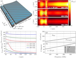
Their structure is simple in concept but challenging to execute, so they first did full-wave simulations using CST Studio Suite to model the optical-tunneling process for verification and sensitivity to imperfections. The silicon waveguide is separated from the adjacent dielectric slab by a narrow air gap (Fig. 1). The silicon thickness is 200 µm, the waveguide’s width is 160 µm, and the separation is variable. (Interestingly, the entire structure is surrounded by air, with no supporting substrate.)
The propagation of the energy uses the fundamental transverse-electric (TE) mode of the waveguide. In this mode, the electric field vector is parallel to the slab plane. In the absence of the slab, all of the energy would be confined within this mode, and no power would be lost to the surrounding space.
However, the slab couples with the evanescent fields of the waveguide’s mode, and thereby captures a portion of confined power, which is then transferred into the fundamental TE0 mode. Evanescent waves or fields are formed when waves traveling in a medium undergo total internal reflection at a boundary (this is the same phenomenon that makes cladded optical fiber so effective for light propagation).
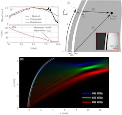
In this way, the terahertz waves are progressively leaked from the waveguide to the slab, a process known as optical tunneling (Fig. 2). The complex propagation constant of the leaky mode describes its dispersion and rate of leakage, parameters that are critical to in-slab beamforming. The magnitude and distribution of the slab-mode beam is engineered by tailoring the separation along the length of the tunneling waveguide.
The Tall Order of Testing
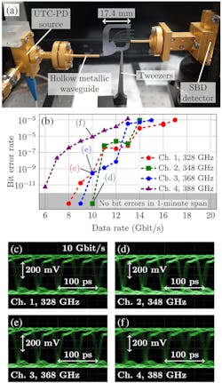
Testing and quantifying the performance of this multiplexer is clearly a major project in itself. The researchers began by optically modulating a two-color infrared laser beam with a nonreturn-to-zero (NRZ) on-off keying pattern using a pseudo-random bit sequence from a pattern generator (Fig. 3). They coupled this to the multiplexer and then coupled and captured its output. A terahertz detector based on a Schottky barrier diode (SBD) was used to extract the modulating signal via envelope detection.
The demodulated pulses were amplified, clipped, and displayed as a classical eye diagram, while a bit-error-rate (BER) tester was used to quantitatively measure the quality of the channel in real-time. For each channel, the center frequency was chosen as a carrier, the data rate was swept in increments of 1 Gbit/sec, and the resultant BER was measured. Data rates of several gigabits per second were supported by each channel.
The complex optical-physics theory and analysis supporting the project, along with more details of the device, its implementation, and the testing are clearly explained in their in-depth and readable nine-page paper “Gratingless integrated tunneling multiplexer for terahertz waves” published in Optica from the Optical Society of America. It’s supported with additional analysis, including efficiency, thermal stability, and crosstalk—all critical performance attributes—in the posted ten-page Supplement.
About the Author

Bill Schweber
Contributing Editor
Bill Schweber is an electronics engineer who has written three textbooks on electronic communications systems, as well as hundreds of technical articles, opinion columns, and product features. In past roles, he worked as a technical website manager for multiple topic-specific sites for EE Times, as well as both the Executive Editor and Analog Editor at EDN.
At Analog Devices Inc., Bill was in marketing communications (public relations). As a result, he has been on both sides of the technical PR function, presenting company products, stories, and messages to the media and also as the recipient of these.
Prior to the MarCom role at Analog, Bill was associate editor of their respected technical journal and worked in their product marketing and applications engineering groups. Before those roles, he was at Instron Corp., doing hands-on analog- and power-circuit design and systems integration for materials-testing machine controls.
Bill has an MSEE (Univ. of Mass) and BSEE (Columbia Univ.), is a Registered Professional Engineer, and holds an Advanced Class amateur radio license. He has also planned, written, and presented online courses on a variety of engineering topics, including MOSFET basics, ADC selection, and driving LEDs.


