Integration Tips for FPC Antennas

This article is part of the TechXchange: Device-Level Antenna Selection Considerations.
This article appeared in Electronic Design and has been published here with permission.
What you’ll learn:
- SMD antennas and FPC antennas have different implications for PCB design.
- Design tips for FPC antennas.
This article explores the design and integration implications for flexible-printed-circuit (FPC) antennas. The FPC is an alternative to a chip antenna and can be an interesting choice for specific embedded designs.
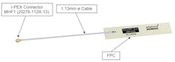
FPC antennas are thin, typically just 0.15 mm, and have a peel-back strip plus an adhesive area to fix them inside a small electronic device in various configurations (Fig. 1). They’re supplied complete with a cable and a connector to attach them to the underside covering or housing of a manufacturer’s electronic product. An FPC is lightweight, probably less than 0.5 g.
Advantage: No Ground Plane Concerns
The FPC works differently than a surface-mount device (SMD) chip antenna. An SMD antenna, which utilizes the ground plane where it’s mounted to radiate, works on the reciprocity principle. A dipole antenna uses two radiators where the length of each radiator is related to the wavelength of the frequency used by the antenna uses. Embedded antennas have one radiator within their mass, and they use an area on the PCB as their counterpoise—commonly referred to as the ground plane.
With an SMD antenna, the length of the ground plane is directly related to the antenna’s wavelength. The correct ground-plane length must be provided in the design so that the antenna is able to operate and perform with good efficiency.
FPC antennas are different in this respect—they don’t require a ground plane to radiate. As such, they allow the designer more freedom to arrange the components in the circuit within the design.
However, it’s important to remember that the coax cable becomes part of the antenna. Thus, the routing of the cable should be designed with care to keep this part of the antenna away from other components that might create noise and interference.
Placement
Because the ground plane isn’t a design consideration for the FPC antenna, the size of the host PCB isn’t a factor as it is with SMD or chip antennas. However, the placement of the FPC antenna still needs to follow some basic rules, since most antennas are sensitive to their environment.
The antenna will radiate in six spatial directions (Fig. 2). Ideally, a minimum of three to five of these directions should be free from obstructions, which will allow the antenna to operate effectively. For the other directions that have obstacles in the radiation paths, there should still be a minimum clearance, which will be defined in the antenna manufacturer’s datasheet.
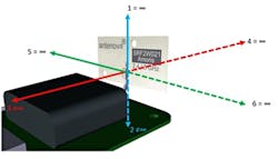
The plastic case for the device will not act as an obstruction unless the material used to manufacture the case is glass filled or if metallic paint has been applied. Metal objects and components such as data cables and printed circuit boards (PCBs) in close proximity to the FPC antenna are usually the culprits that block the signals.
Orientation of FPC
The shape of the device will determine the ideal orientation of the FPC with respect to the host PCB. The antenna’s position in relation to the PCB will depend on the proximity of the ground (Fig. 3).
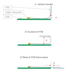
Whichever option is chosen, the distance (d) becomes a critical dimension in the design. This will be specified in the antenna manufacturer’s datasheet.
Device Integration Example
Figure 4 shows an integration example for an FPC antenna. The device has the major components within an outer case. The FPC has been adhered to the inside of the device’s plastic housing, with the cable routed along the PCB so that it will not interfere with any other component. In this case, the FPC was placed on the same plane relative to the PCB. Due to the slim design of the device, this was the optimal location for the antenna.
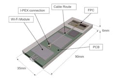
The antenna’s I-PEX cable connects it into the design. All of the transmission lines within the product are designed to have a characteristic impedance of 50 Ω and should be kept as short as possible. All other parts of the RF system, such as transceivers and power amplifiers, should also be designed to have an impedance of 50 Ω.
We recommend using a commercial RF design package to create the transmission-line layout, taking into account the PCB thickness, copper thickness, and the dielectric constant. The program will calculate the recommended width for the transmission line, and the appropriate spaces between the reference ground plane on either side of the antenna feed trace to keep the 50-Ω system impedance.
Is an FPC Antenna Good for Your Design?
SMD antennas may be the most obvious choice for a small PCB, but FPC antennas are widely used in applications where there’s insufficient space for a SMD antenna.
Off-the-shelf FPC antennas aren’t recommended for the very smallest devices, but there are plenty of applications where FPCs can work well. They can be a particularly useful choice for those designs where ground-plane length and space are restricted.
Remember that FPCs aren’t compatible with pick-and-place machines. However, they’re a good choice for lower-volume manufacturing in which devices are assembled by hand.
For more TechXchange articles on this topic CLICK HERE.
To see TechXchange pages on other topics CLICK HERE.
About the Author
Geoff Schulteis
RF Antenna Application Specialist, Antenova Ltd.
Geoff Schulteis is an RF Antenna Application Specialist, at Antenova Ltd. Geoff leads technical support for Antenova’s North American customer designs. He’s an Antenna Engineering professional with more than 20 years’ experience in designing, integrating, and testing antenna systems for consumer products from R&D, through manufacturing & commercial deployment. Geoff is uniquely familiar with the wireless product development landscape and has designed antennas for various IoT applications utilizing protocols ranging from 2G through 5G, earning him multiple patents.
