A Robust, Large-Signal Model for LDMOS RF Power Transistors
Download this article in .PDF format
When modeling transistor behavior, models can generally be divided into three categories: physical, empirical, and behavioral. Each has its own advantages and disadvantages, making it more or less suitable for modeling different types of transistors for different applications.
The physical model is at one side of the spectrum. Although it is complex, it relates to the physics and layout of the device. Thus, the physical model generates physical insight and is inherently suitable for statistical analysis. At the other side of the spectrum is the behavioral model, a black box that is easily extracted and represents measured data (S-parameters or X-parameters).
A compromise in terms of functionality, ease of extraction, and robustness is offered by the empirical model. It is generally some form of compact model with physical components described by non-physical fitting functions. The suitability of this model to describe the performance in the region outside of where the model was extracted depends both on the extraction method and the formulas used in the model.
Ampleon has chosen to develop its own empirical models for the newest LDMOST technologies. This development has been driven by the fast time-to-market needs of these models, which are intended to provide accurate simulation results for the targeted applications.
Ampleon LDMOST technology is primarily aimed at base-station applications. In the early days, LDMOST operated in Class AB in feed-forward systems. Today, two- or three-way Doherty amplifiers in combination with digital pre-distortion (DPD) systems are the norm for efficient base stations. To enable accurate modeling of the Doherty configuration, modeling the Class C behavior of the LDMOST is crucial. Therefore, a focus was placed on this aspect while extracting and generating the new model.
This article describes the extraction and performance of the core model. Three power amplifiers (PAs) in a Doherty configuration are then simulated. The results are shown to illustrate the model performance and usability of these models for a Doherty design.
Extraction Flow and Methodology
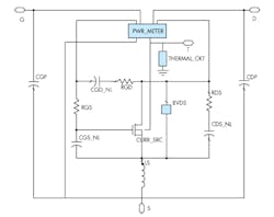
The extraction flow is based on current-voltage (IV) curves over temperature, S-parameters, and large-signal RF performance in the region where the model should describe the transistor behavior accurately. The current source, extrinsic parasitics, and intrinsic parasitics are then extracted (Fig. 1).
All measurements are performed on wafer. Thus, the de-embedding needed to obtain the response of the LDMOST by itself is minimized. Measuring an unpackaged transistor does limit the size of the LDMOST that can be measured. Ground-signal-ground RF probes, which are needed for accurate measurements, are limited in terms of current- and power-handling capability. Typical gate peripheries of around 6 mm have been used, keeping the number of fingers greater than two in order to avoid extraction of a model based on end-fingers only.
During the model extraction, stringent specs are placed on IV performance, S-parameter accuracy at multiple bias points, and final RF performance accuracy with regard to gain, efficiency, and impedances. When these conditions are met, the model can be successfully used for monolithic microwave integrated circuit (MMIC) design, as well as for discrete power Doherty designs.
In addition, designers and customers can request a special version of the model. With this version, the internal current source (the center of the model in Fig. 1) can be accessed to monitor the internal current and voltage waveforms.
DC Validation
The formulas of the current source are fitted using both non-pulsed and pulsed IV measurements over temperature. Measurements are performed using AMCAD Engineering’s PIV-240-10 pulsed IV solution. The thermal model, which describes the thermal behavior of the device, is also extracted. A multi-section thermal circuit is implemented to capture the thermal time constants in the device.
For large RF power transistors in a package, the thermal behavior is largely dominated by the thermal characteristics of the die’s surroundings. Therefore, the internal thermal circuit can be negated by an external thermal circuit.
The formulas in the current source of the model have been optimized in such a way as to accurately represent the currents in Ampleon’s three latest 28-V LDMOST technologies, as well as in its 50-V LDMOST technology. Figure 2 demonstrates the general fit of all IV curves after fitting the current source parameters.
Due to the non-physical nature of the model, a complete new extraction needs to be done for each new technology. There are no physical parameters in the model that can reflect the process change. However, as stated in the introduction, time-to-market of a model is quite fast for these models, since measurement and extraction of the model is much less complicated compared to physical model extraction.
S-Parameter Validation
The wideband pulsed S-parameters are measured at several bias points covering the total IV plane. The PIV-240-10 is used in combination with an N5242 PNA-X network analyzer for these measurements.
The extrinsic and intrinsic parasitics are extracted and the voltage dependence on the intrinsic parasitics is determined. The modeled trends in the S-parameters over all bias points are verified. Special attention is paid to the Class C and AB bias points.
Load-Pull Validation
Load-pull measurements are used to validate the compact transistor model with the proper load terminations for optimal RF performance. The impedances presented to the transistor are varied in such a way that the generated load plane includes the maximum efficiency and the maximum power load states. A comparison is made between measured and modeled RF performance. To obtain an overall good fit for both small- and large-signal performance of the model, the extrinsic and intrinsic parasitics are fine-tuned in an iterative optimization process.
Measurements are performed using Maury Microwave’s MT2000 active load-pull system. In the system at Ampleon today, the fundamental and second harmonic source and load terminations can be controlled, while the third harmonic terminations are only measured. To keep the accuracy of the measured environment, these measured fundamental, second, and third harmonic terminations are presented to the model when comparing the measured and the modeled RF performance.
Special emphasis is placed on the actual frequency of operation of the transistor during extraction. However, a wider frequency range is also verified. Stringent specs are again placed on the RF performance of the model.
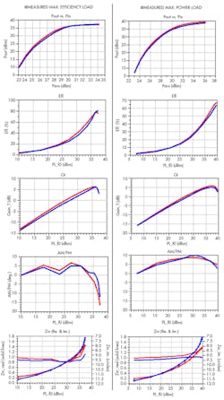
Performance is verified for Class AB bias (Vd = 28 V) and for Class C bias (Vg = 0.3 V, Vd = 28 V). Gain, efficiency, power, AM/PM, and input impedance are verified at the maximum efficiency and maximum power load states. Fig. 3 shows the results for Class C operation. Furthermore, a tradeoff occurs between the simulated load-pull contours and the power efficiency.
The model performance is verified over a wider frequency range, demonstrating good behavior for both Class AB and Class C operation. Optimal load impedances are predicted by the model and the input impedance is modeled accurately. This very good prediction of the active device will allow designers to generate amplifier products—both discretes and MMICs—as described in the next sections.
3-Way Discrete Doherty Design Modeling
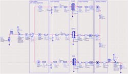
Combining the core model with bond-wire and package models enables the generation of accurate models of packaged power RF transistors. This led to the design of a 3-way Doherty (Fig. 4).
The model of the BLC9G20LS-120V transistor is used to assess the feasibility of a 3-way Doherty with high performance in the frequency band from 1,805 to 1,880 MHz. Matching of the transistor is realized with ideal microstrip lines. Some realistic losses are added in order to characterize insertion losses on a standard printed-circuit board (PCB). The fast simulation time of this model made it possible to fine-tune the amplifier for maximum performance.
The output combiner and input splitter are added to simulate the complete Doherty behavior. The peaking amplifiers are biased to attain the desired turn-on. The input phase is adjusted to allow the three branches to power-combine in phase.
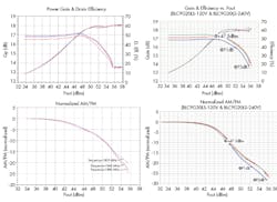
This Doherty architecture has been implemented in a real circuit with the BLC9G20LS-120V transistor used to create the main amplifier, while the BLC9G20LS-240PV transistor is used to create both peaking amplifiers in a push-pull package.
Figure 5 shows both simulated and measured gain, efficiency, and AM/PM. It can be seen that the behavior is very similar and the absolute values are also quite close. This validates that the device model is suitable to study a complex architecture like a 3-way Doherty.
2-GHz Integrated Doherty MMIC Modeling
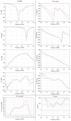
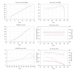
In addition, using passive MMIC components that have been validated in a separate process allows designers to derive an integrated Doherty MMIC, such as the BLM8D1822S-50PBG, with a very good level of predictability. This capability is illustrated in Figs. 6 and 7 for small- and large-signal operation, respectively.
A good match between modeled and measured data is observed for both ON and OFF states in small-signal operation, with special attention given to S22 and K-factor prediction. The same level of correlation is obtained in large-signal operation, taking into account parameters like gain, efficiency, output power, and AM/PM while also looking at input and output impedance prediction.
Conclusion
Compact transistor modeling is the most crucial step in a successful design flow. It can lead to first-pass design success and faster time-to-market when used in conjunction with circuit simulators. Ampleon’s new empirical LDMOST model has proven to be very accurate. The IV behavior over temperature is characterized well, as are predictions for the S-parameters. While main emphasis is placed on the S-parameters at Class AB and C bias points, S-parameters are well characterized at different bias points, too.
Characterizing the load-pull behavior at RF frequencies is most important. The model is optimized for several frequency ranges of application, satisfying stringent specs with regard to gain, efficiency, power, and impedance levels. Other important qualities of the model are its ease of extraction and its robustness with the ADS and Microwave Office circuit simulators. The Ampleon model is therefore suitable for modeling high-power discrete designs, as well as medium-power MMIC designs. The model is especially well suited for Doherty amplifiers because of its high level of Class C prediction.
As was shown, the AM/PM prediction of the model is quite accurate. The model also predicts distortion very well when excited by two tones. Investigations are still ongoing in this area. Harmonic load-pull accuracy is under examination as well. Lastly, breakdown phenomena are currently only implemented very crudely into the model. This is another area to be investigated in the future.
