CMOS LNA Aids UWB Receivers
This file type includes high resolution graphics and schematics when applicable.
The broad swath of spectrum (7500 MHz) allocated by the United States Federal Communications Commission (FCC) in 2002 in the 3.1 to 10.6 GHz range creates many opportunities for new communications systems and their components.1 The benefits of such ultrawideband (UWB) radios include low-power operation, high data rates (to 1 Gb/s), reduced interference, and low cost.
One of the key component blocks in these radios is the low-noise amplifier (LNA), which must meet several stringent requirements—including broadband input matching, flat and high power gain, low noise figure, high linearity, and low power consumption. The design of such an amplifier can be a great aid to these UWB radios and systems.
A number of UWB LNAs have been developed based on CMOS technology.2-8 The distributed amplifier (DA) has been one of the more popular architectures for this application. Since DA LNAs provide good wideband input matching, flat gain, and generally high input third-order intercept (IIP3) performance, they are well suited to these UWB applications.2-4 But DA LNAs consume a great deal of power with relatively low power gain in a large chip area.
Resistive feedback is a good solution for obtaining wide bandwidth and flat power gain.5-7 However, the use of a resistor in the feedback path reduces the power gain and degrades noise performance. One recent LNA topology of note is the cascode configuration with a Chebyshev input matching filter, which provides good wideband input matching and high power gain8; however, the noise figure is degraded by the filter’s insertion loss.
One challenge for UWB LNAs is posed by the linearity requirements, owing to the large numbers of in-band interference sources in that frequency range and the cross-modulation/intermodulation caused by blockers or transmitter leakage in a reconfigurable receiver.9 Furthermore, while the transmit frequency (fT) increases with technology scaling, linearity tends to degrade due to lower supply voltages in use and high-field mobility effects.9 This makes wideband linearization important.10,11
Linearization techniques which optimize overdrive voltage (Vgs - Vth) can be used to obtain peak IIP3. However, the bias voltage range for peak IIP3 is narrow, so that boosting linearity can be sensitive to process variations. The derivative super-position (DS) method12-14 uses an additional transistor’s nonlinearity to cancel that of the main device; it involves MOS transistors working in triode12 or in the weak inversion region13,14.
Therefore, using the DS method, it is difficult to match the transistors working in different regions, resulting in a linearity improvements that are highly sensitive to variations in pressure volume and temperature (PVT). The body biasing technique15 is suitable for improving linearity performance; unfortunately, it degrades gain and noise performances. In ref. 16, the post-distortion technique was used to improve linearity, with good results.
To achieve good performance for UWB systems, a common-gate (CG) LNA design is proposed. These LNAs offer simple input matching networks with good linearity and low power consumption compared to common-source (CS) LNAs. Because the power gain of a CS LNA tends to be low,17 a CS amplifier is used in this design as a second stage. The proposed LNA design employs current-reuse and forward body biasing techniques to achieve low power consumption. In addition, shunt-series peaking techniques are used to extend the 3-dB bandwidth, and a post-distortion technique is employed to improve the linearity performance.
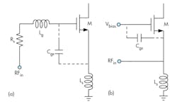
Based on their input matching characteristics, reported CMOS UWB LNA architectures can be divided into two major groups: CS and CG LNAs.18Figure 1 offers the two general topologies for these amplifier types. Figure 1(a) is a CS LNA that requires at least two inductors (Lg and Ls) for simultaneous noise and input matching (SNIM). Assuming the channel resistance, γ0, and the gate-drain parasitic capacitance, Cgd, are negligible, the CS LNA’s quality factor (Q) can be derived as:
Substituting Eq. 2 into Eq. 1 yields Eq. 3:
where:
ω0 = the resonant angular frequency of the input impedance;
gm = the transconductance of the metal-oxide-semiconductor field-effect transistor (MOSFET);
Lg = the gate inductor;
Ls = the source inductor; and
Cgs = the gate-source parasitic capacitance of the device.
The architecture is inherently narrowband because of the high Q value and the difficulty in achieving wideband input match to the signal source in the presence of the parasitic capacitances. Figure 1(b) shows a typical CG LNA. The input matching network of the CG LNA has a parallel resonance, and the Q of the CG LNA can be expressed as:By substituting Eq. 5 into Eq. 4, QCG can be expressed by Eq. 6:
Since Ls is intended to block the RF leakage to the ground, the Ls value of a conventional CG LNA is higher than that of a CS LNA, and the Qcs value is higher than the Qcg value. Obtaining a wideband input match and absorbing parasitic capacitances with a CG LNA is relatively simple, making this a suitable topology for UWB applications.
This file type includes high resolution graphics and schematics when applicable.
Cutting Power Consumption
This file type includes high resolution graphics and schematics when applicable.
Mobile and portable applications require low power consumption, and the most efficient approach for reducing power consumption is through power supply voltage scaling. In the proposed LNA circuit, the forward body biasing technique is employed to reduce the threshold voltage, Vth. The Vth for a MOSFET can be found from Eq. 7:
where:
Vth0 = the threshold voltage when Vbs = 0;
γ = the body-effect coefficient;
σf = the surface potential; and
Vbs = the voltage between the body and the source.
Usually, Vbs ≤ 0, so Vth ≥ Vth0. To reduce Vth, Vbs is set greater than zero so that Vth < Vth0. The typical value of Vth is about 0.5 V. For the proposed LNA design, Vbs = 0.29 V and Vth = 0.43 V.
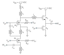
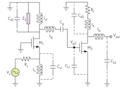
The UWB LNA was designed and simulated in a standard 0.18-μm RF CMOS process. Figure 3 shows a schematic diagram of the proposed LNA, including the output buffer stage (M4, M5). The current-reuse configuration can be considered as a two-stage cascade amplifier, where the first stage is the CG amplifier (M1) and the second stage is the CS amplifier (M2).
The signal amplified by M1 is coupled to the gate of M2 by series resonance (Lg and Cg) while the source of M2 is bypassed by capacitor Cb. Besides, Cb determines the low-frequency band expansion and gain flatness. The circuit saves power through the reuse of the bias current.
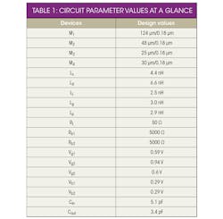
The CG topology LNA exhibits low power gain, so a CS amplifier is included in the second stage. It employs a gain peaking technique which consists of RL, LL, M2, and Lp. To reduce the threshold voltage of the transistor, the forward body biasing is employed. The post-distortion technique is used in the first stage (M3), reducing the nonlinearity of the main device (M1). Table 1 summarizes the circuit parameters of the proposed LNA.
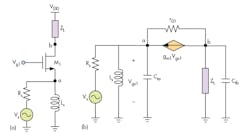
RF/microwave components and systems are typically designed for a standard impedance of 50 Ω, so the input stage of the UWB LNA should match to 50 Ω with minimal power reflection.21 For simplicity in this analysis, body effects are ignored. Figure 4 shows the CG input stage of the proposed UWB LNA, and the input impedance can be derived by Eq. 8:
where:
Cta = the total capacitance at node a;
Ctb = the total capacitance at node b;
Cgs1 = the gate-to-source capacitance;
gm1 = the transconductance;
r01 = the output resistance of M1; and
ZL = the CS stage equivalent load impedance.
As Eq. 8 indicates, the input impedance approximates 1/gm1 over the frequency band of interest. Transconductance gm3 << gm2, where gm2 and gm3 are the transconductances of transistor M2 and M3, respectively. The input impedance Zin(ω as seen from resistor Rs of the CG LNA is about the same with or without transistor M3 present, so that M3 cannot be considered to significantly affect the input impedance matching.
However, for a wideband input match, Eq. 8 indicates that gm1 of M1 in the CG stage should slightly exceed 20 mS. Through simulation, input matching is considered good when gm1 approaches 26 mS.
The achievable maximum power gain also depends on the output impedance matching. In the proposed LNA, a simple source follower, which consists of M4 and M5, is employed to obtain output impedance matching. If the source of M2 is perfectly grounded by Cb, the equivalent schematic of the proposed LNA can be redrawn in Fig. 5, where the proposed UWB LNA is created by the two-stage amplifier.
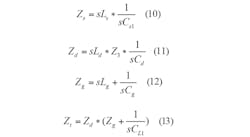
The first stage is a CG amplifier and the second stage is a CS amplifier. For simplicity, body effects are not considered. The voltage gain of the first stage, AV1, can be expressed by Eq. 9:
where:
gm1 = the transconductance of M1;
r01 = the channel resistance of M1;
RS = the input source resistance (50 Ω);
Cs1 = the source parasitic capacitance caused by Cgs1;
Cd1 = the drain parasitic capacitance caused by Cgd1;
CL1 = the parasitic load capacitance of the second stage; and
Z3 = the equivalent impedance of M3.
For simplicity’s sake, the direct-current (DC) blocking capacitors Cin and Cout are ignored in the analysis.
The voltage gain of the second-stage, AV2, is given by Eq. 14:
gm2, γ02, and CL2 are the transconductance of transistor M2, the channel resistance of M2, and the total load capacitance at the second-stage output, respectively. Additionally, Cd2 is the calculated parasitic capacitance at the drain of M2, which is produced by the gate-to-drain parasitic capacitor (Cgd2). The overall circuit frequency response of S21 has a good flatness and a high power gain because of the cascaded first and second stages.
This file type includes high resolution graphics and schematics when applicable.
A Closer Look
This file type includes high resolution graphics and schematics when applicable.
which are produced by source resistor Rs and the channel noise of M1, M2, and load resistor RL. Parameters k, T, γ, and Δf represent Boltzmann’s constant, the absolute temperature (in degrees Kelvin), the thermal noise coefficient (having a value from 1 to 2 in the saturation region of a short channel MOSFET), and the noise bandwidth (in Hz), respectively.
The noise factor of the proposed LNA can be expressed by Eq. 21:
where V2n,out is the total noise at the output and AV is the total voltage gain.
The total voltage gain AV can be obtained by Eqs. 17 and 21. From Eq. 21, it can be seen that the effects of gm1 and gm2 can be seen on achieving a lower noise factor; for low noise and low power consumption, gm1 should have a low value. But this can also have adverse effects on the total noise factor since low gm1 leads to low first-stage gain.
Alternately, from Eq. 21, it can be seen that a high gm2 value is beneficial for low noise factor, although the high value will also increase power dissipation. For best performance, the values of gm1 and gm2 should be optimized. Because both transconductance values depend on transistor width (W1 and W2, in the proposed LNA design, the optimal values of W1 and W2 are 124 and 48 μm, respectively.
The proposed UWB LNA was designed and simulated with the aid of the Advanced Design System (ADS) software from Agilent Technologies (now Keysight Technologies), using a standard 0.18-μm silicon RF CMOS process. With current reuse and forward body biasing, the supply voltage is only +1.3 VDC and the power consumption is only 3.1 mW.
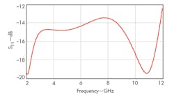
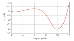
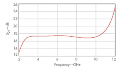
Figure 6 shows simulated input reflection coefficient (S11, which is less than -13 dB from3 to 11 GHz. Figure 7 shows simulated output reflection coefficient (S22), which is less than -14 dB from 3 to 11 GHz. Figure 8 shows voltage gain (S21) for the LNA, which ranges from 16.8 to 18.9 from 3 to 11 GHz. As a result of a shunt-series peaking technique, S21 shows high voltage gain with good flatness.
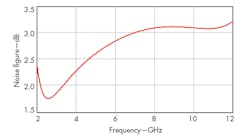
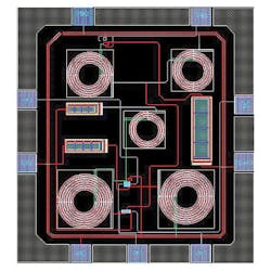
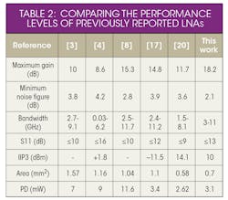
Figure 9 plots the noise figure of the proposed LNA, which ranges from 1.9 to 3.2 dB across 3 to 11 GHz. Figure 10 shows the layout of the proposed LNA, with total chip area of 0.87 × 0.81 mm2, including the input and output pads. Table 2 summarizes its performance and compares it with previous work.
Acknowledgment
The authors would like to thank the research platform of the Open Fund Project for access to the coal mine monitoring network based on the wireless sensor networks in the Department of Education of Hunan Province, grant No. 12C0986.
Xu Xia, Professor
Hunan Vocational College of Security Technology, Changsha, 410151, Hunan Province, People’s Republic of China
Fengying Han, Professor
Changsha Aeronautical Vocational and Technical College, Changsha, 410014, Hunan Province, People’s Republic of China
This file type includes high resolution graphics and schematics when applicable.
References
This file type includes high resolution graphics and schematics when applicable.
1. G. Roberto Aiello and Gerald D. Rogerson, “Ultra-wideband Wireless Systems,” IEEE Microwave Magazine, June 2003, pp. 36-47.
2. Ren-Chieh Liu, Chin-Shen Lin, Kuo-Liang Deng, and Huei Wang, “A 0.5-14-GHz 10.6-dB CMOS Cascode Distributed Amplifier,” in IEEE International Symposium on Very Large Scale Integrated (VLSI) Circuits Digest of Technology Papers, December 2003, pp. 139-140.
3. Yueh-Hua Yu, Yi-Jan Emery Chen and Deukhyoun Heo, “A 0.6-V Low Power UWB CMOS LNA,” IEEE Microwave and Wireless Components Letters, Vol. 17, No. 3, March 2007.
4. Frank Zhang, and Peter Kinget, “Low Power Programmable-Gain CMOS Distributed LNA for Ultra-Wideband Applications,” IEEE International Symposium on Very Large Scale Integrated (VLSI) Circuits Digest of Technology Papers, June 205, pp. 78-81.
5. Herbert Knapp, Dietmar Zoschg, Thomas Meister, Klaus Aufinger, Sabine Boguth, and Ludwig Treitinger, “15 GHz Wideband Amplifier with 2.8 dB Noise Figure in SiGe Bipolar Technology,” IEEE International Symposium on Radio Frequency Integrated Circuits (RFIC), 2001, Digest of Technology Papers, pp. 287-290.
6. Stefan Andersson, Christer Svensson, and Oskar Drugge, “Wideband LNA for a Multistandard Wireless Receiver in 0.18 μm CMOS,” IEEE Solid-State Circuits Conference, September 16-18, 2003, pp. 655-658.
7. Ranjit Gharpurey, “A Broadband Low-Noise Front-End Amplifier for Ultra Wideband in 0.13 um CMOS,” IEEE Custom Integrated Circuits Conference, October 3-6, 2004, pp. 605-608.
8. J.Y. Lee, J.H. Ham, Y.S. Lee, and T.Y. Yun, “CMOS LNA for full-band ultra-wideband systems using a simple wide input matching network,” IEEE Transactions on Microwave Antennas & Propagation, Vol. 4, No. 12, December 2010, pp. 2155-2159.
9. Wei-Hung, Gang Liu, Boos Zdravko, and Ali M. Niknejad, “A Highly Linear Broadband CMOS LNA Employing Noise and Distortion Cancellation,” IEEE Journal of Solid-State Circuits, Vol. 43, No. 5, May 2008, pp. 1164-1176.
10. Sudip Shekhar, Jeffrey S. Walling, and David J. Allstot, “Bandwidth Extension Techniques for CMOS Amplifiers,” IEEE Journal of Solid-State Circuits, Vol. 41, No. 11, November 2006, pp. 2424-2439.
11. Vladimir Aparin, Gary Brown, and Lawrence E. Larson, “Linearization of CMOS LNA’S Via Optimum Gate Biasing,” International Symposium on Circuits and Systems (ISCAS), Vol. 4, May 23-26, 2004, pp. 748-751.
12. Yong-Sik Youn, Jae-Hong Chang, Kwang-Jin Koh, Young-Jae Lee, and Hyun-Kyu Yu, “A 2 GHz 16dBm IIP3 Low Noise Amplifier in 0.25-μm CMOS Technology,” IEEE Conference on Solid-State Circuits, Vol. 1, 2003, pp. 452-507.
13. Vladimir Aparin and Lawrence E. Larson, “Modified Derivative Superposition Method for Linearizing FET Low-Noise Amplifiers,” IEEE Transactions on Microwave Theory and Techniques, Vol. 53, No. 2, February 2005, pp. 571-581.
14. Tae Wook Kim, “A Common-Gate Amplifier With Transconductance Nonlinearity Cancellation and Its High-Frequency Analysis Using the Volterra Series,” IEEE Transactions on Microwave Theory and Techniques, Vol. 57, No. 6, June 2009, pp. 1461-1469.
15. Aya Mabrouki, Thierry Taris, Yann Deval, and Jean Baptiste Begueret, “CMOS Low-Noise Amplifier Linearization through Body Biasing,” IEEE International Symposium on Radio Frequency Integration Technology (RFIT), January 2009, pp. 150-153.
16. Namsoo Kim, Vladimir Aparin, Kenneth Barnett, and Charles Persico, “A Cellular-Band CDMA 0.25-μm CMOS LNA Linearized Using Active Post-Distortion,” IEEE Journal of Solid-State Circuits, Vol. 41, No. 7, July 2006, pp. 1530-1534.
17. J.-Y. Lee, H.-K. Park, H.-J. Chang, and T.-Y. Yun, “Low-power UWB LNA with common-gate and current-reuse techniques,” IEEE Transactions on Microwave Antennas & Propagation, Vol. 6, No. 7, May 2012, pp.793-799.
18. Muhammad Khurram and S.M. Rezaul Hasan, “A 3-5 GHz Current-Reuse gm-Boosted CG LNA for Ultrawideband in 130 nm CMOS,” IEEE Transactions on Very Large Scale Integration (VLSI) Systems, Vol. 20, No. 3, March 2012, pp. 400-409.
19. Heng Zhang and Edgar Sanchez-Sinencio, “Linearization Techniques for CMOS Low Noise Amplifiers: A Tutorial,” IEEE Transactions on Circuits and Systems, Vol. 58, No. 1, January 2011, pp. 22-36.
20. Heng Zhang, Xiaohua Fan, and Edgar Sanchez Sinencio, “A Low-Power, Linearized, Ultra-Wideband LNA Design Technique,” IEEE Journal of Solid-State Circuits, Vol. 44, No. 2, February 2009, pp. 320-330.
21. P. Andreani and H. Sjoland, “Noise optimization of an inductively degenerated CMOS low noise amplifier,” IEEE Transactions on Circuits and Systems-II: Analog and Digital Signal Processing, Vol. 48, No. 9, September 2001, pp. 835-841.
This file type includes high resolution graphics and schematics when applicable.
