MMIC PIN-Diode Limiters Operate to 20 GHz
This file type includes high resolution graphics and schematics when applicable.
To prevent damage to highly sensitive receiver front ends, limiters are used to sink extra RF power away from sensitive circuits. Limiter circuitry performs as a low-loss, broadband, and compact component. PIN diodes are attractive devices for limiter design, as they enable key performance features while exhibiting high power handling. Plextek offers an application note detailing a design example of a monolithic-microwave-integrated-circuit (MMIC) PIN-diode limiter labeled, “Technology Overview: Broadband, Low-Loss Limiter MMICs.”
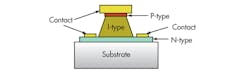
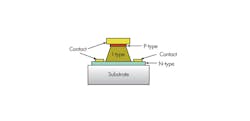
PIN diodes are offered in discrete packages or integrated into IC processes. The benefit of using an integrated PIN diode for limiter design is the elimination of packaging parasitics, which degrade the receiver’s noise performance. PIN diodes are built from an intrinsic (I) region of high resistivity in between a P-type and N-type semiconductor.
When the PIN-diode structure is forward biased, carriers are injected into the I region. The resistance of the region is lowered as a result. This unique response enables a PIN diode to operate as a current-controlled resistor and switch at RF/microwave frequencies. Imperfections in the diode’s I region cause charge accumulation, which generates a direct-current (DC) rectified from the RF signal. A DC return path is necessary for proper function of the limiter.
An example of the design and simulation of a fifth-order limiter modeled after a fifth-order low-pass filter (LPF) is provided in the application note. The shunting configuration of the diodes uses a back-to-back approach composed of antipodal pairs. This method allows for operation from 0.5 to 20.0 GHz. An LPF structure designed to absorb the parasitic capacitance of the zero-biased diode pairs increases the limiter’s broadband capability. Integrated DC-blocking metal-insulator-metal (MIM) capacitors are used at the RF input and output. The low-pass filter also comprises high-impedance metal tracks for constructing inductors.
An electromagnetic (EM) simulation using practical bond-wire parasitics yields return-loss of greater than -18 dB above 2 GHz. Return-loss degrades to -13 dB below 500 MHz. To simulate the operation of the limiter in a small-signal method, the forward conduction state is triggered by a high-level RF signal. The diodes are then switched to the DC-induced forward bias state. The power handling of the limiter typology is dictated by the power-handling capability of the primary diodes. For this typology, which is implemented with TriQuint’s VPIN process, it is suggested that the structure can handle continuous-wave (CW) power of 5 W.
As foundries may not offer a large-signal model of a PIN diode, modeling a limiter could be difficult. Plextek generated a large-signal model to determine the benefits of simulating the limiter system. The results at 2, 10, and 18 GHz were reported with small variations caused by frequency shifting. The limiter delivers +17 to +18 dBm saturated output power. The complex power characteristic of these power limiters also produces a distinct drop, or kink, after reaching a peak power level. Although the large-signal model does not report this, it does properly represent the peak power level.
Plextek Ltd., London Road, Great Chesterford, Essex CB10 1NY UK, +44 (0) 1799 533200.
This file type includes high resolution graphics and schematics when applicable.
About the Author
Jean-Jacques DeLisle
Jean-Jacques graduated from the Rochester Institute of Technology, where he completed his Master of Science in Electrical Engineering. In his studies, Jean-Jacques focused on Control Systems Design, Mixed-Signal IC Design, and RF Design. His research focus was in smart-sensor platform design for RF connector applications for the telecommunications industry. During his research, Jean-Jacques developed a passion for the field of RF/microwaves and expanded his knowledge by doing R&D for the telecommunications industry.
