
This file type includes high resolution graphics and schematics when applicable.
Integration is a goal for many wireless electronic products, with more and more capabilities being packed into ever-smaller equipment housings. When it makes sense, multiple functions can be incorporated into a single component housing to save space in the final product design. Such is the case with the model TSS-53LNB+ low-noise amplifier (LNA) from Mini-Circuits.
This compact surface-mount unit doesn’t just incorporate an amplifier capable of high gain and low noise figure from 0.5 to 5.0 GHz: It also provides a switchable bypass circuit, which can be selected in the presence of large signals to avoid overdriving the LNA’s sensitive input port. As with any of the firm’s products, the amplifier is extremely competitively priced for use in a wide range of multiple-tuner and other wireless-communications applications.
The model TSS-53LNB+ LNA (Fig. 1) is based on a 0.25-μm enhancement-mode GaAs pseudomorphic-high-electron-mobility-transistor (pHEMT) semiconductor process. It uses a Darlington cascode configuration to achieve flat gain across a wide bandwidth, with reliable operation from a standard +5-VDC supply. It typically draws about 80 mA current from that supply, and the amplifier is also enabled by means of a +5-VDC voltage.
The bypass LNA is usable from 0.5 to 5.0 GHz, with 21.5-dB typical gain at 2 GHz and 1.3 dB typical noise figure at 2 GHz. It provides +21-dBm typical output power at 1-dB compression at 2 GHz—with ±0.7 dB flat gain from 700 to 2100 MHz—with no matching components.
The amplifier circuitry is powered down in bypass mode to conserve power. The LNA was designed with input and output impedances as close to 50 Ω as possible so that additional external impedance-matching components would not be required for optimum performance. Suitable for test-and-measurement and wireless-communications applications, the RoHS-compliant bypass LNA is supplied in a surface-mount 12-lead 3 × 3 mm MCLP package complete with on-die electrostatic-discharge (ESD) protection, per Class 1A requirements [of the 250-V Human Body Model (HBM)]. The package boasts Sn-Ag alloy over Ni lead finish for good thermal performance over a wide operating temperature range (-40 to +85°C).
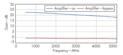
The amplifier’s performance was characterized in both normal amplifier and bypass modes using a model PNA-X RF/microwave vector network analyzer (VNA) from Agilent Technologies. The amplifier was found to be extremely stable, with better than 30 dB isolation from about 300 to 6100 MHz (sufficient bypass isolation is critical to achieving high amplifier stability). Arguably as impressive as the amplifier’s flat gain across frequency—typically about 21.5-dB gain at 2 GHz, with gain flat within ±0.7 dB from 0.7 to 2.1 GHz—is the amplifier’s response in bypass mode (Fig. 2), in which the gain/loss is flat within a fraction of a decibel below 0 dB from 0.5 to 5.0 GHz.
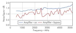
Similarly, the amplifier delivers impressive noise-figure performance (Fig. 3) in both active and bypass modes. With the amplifier active, the noise figure reaches about 1.2 dB at 1 GHz and 1.3 dB at 2 GHz, with about 1.5 dB noise figure at 3 and 4 GHz, and peaking at a level of about 1.8 dB at 5 GHz. In the bypass mode, the noise figure remains below its rated specification for the full operating bandwidth. The measured noise figure in bypass mode is a low 0.7 dB at 1 GHz and 0.9 dB at 2 GHz, with noise figure of about 1.0 dB at 3 GHz—reaching only 1.4 dB at 4 GHz and 1.1 dB at 5 GHz.
This file type includes high resolution graphics and schematics when applicable.
Noteworthy Output
This file type includes high resolution graphics and schematics when applicable.
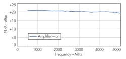
The amplifier’s output characteristics, such as output power at 1-dB compression and output third-order intercept point (OIP3), are quite respectable for an amplifier that also helps enhance receiver sensitivity. The specified output power at 1-dB compression is +21 dBm at 2 GHz, and the measured performance remains flat above +20 dBm from 0.5 to 5.0 GHz (Fig. 4). The measured OIP3 is +34.8 dBm at 2 GHz (data not shown) and +35.2 dBm at 5 GHz with the amplifier active. It is better than +50 dBm at 2 GHz in bypass mode and better than +44 dBm at 5 GHz in bypass mode.
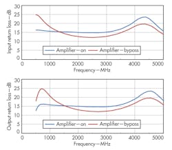
The LVA exhibits good return-loss performance without additional external matching components (Fig. 5). It achieves typical input return loss of 15.5 dB at 1 GHz, 15.0 dB at 3 GHz, 21.2 dB at 4 GHz, and 15.7 dB at 5 GHz. The typical output return loss is 15.5 dB at 1 GHz, 20.4 dB at 2 GHz, 14 dB at 3 GHz, 10.7 dB at 4 GHz, and 9.7 dB at 5 GHz.
To evaluate stability and performance drift that might result from being in the presence of high-level input signals, the amplifier was tested before and after exposure to input signals at 10-dB higher than the rated 1-dB compression point. No change in current from the nominal 80 mA at +5 VDC was found at 100 MHz, 3 GHz, or 6 GHz, using input test power levels of +4.16 dBm at 100 MHz, +1.06 dBm at 3 GHz, and +1.85 dBm at 6 GHz. Testing for variations in gain, noise figure, and current—according to the HBMs at 250 and 500 V—also revealed minimal drift of less than 10%, with only 0.13-dB drift in gain per the HBM at 250 and 500 V, only 0.07-dB drift in noise figure, and no drift (0 mA) in current when the amplifier was tested per the 250- and 500-V HBMs.
Related Articles
• Transceiver Supports 8 × 8 MIMO Systems
• Current Reuse Gains UWB LNA
• Compact LNA Drives 2.5-GHz Base Stations
This bypass LNA allows the active amplifier circuitry to be protected during high-input-signal conditions and to reduce current consumption in communications systems during particular operating conditions. The amplifier’s consistent gain and noise profiles in active and bypass modes imply that a shift from amplified operation to bypass mode can occur without a dramatic change to the system’s power consumption profile. The amplifier is a candidate for any number of mobile applications, including receivers in WiMAX and WLAN systems. In a WLAN network, for example, a bypass mode can be applied to avoid near-field distortion. P&A: $1.28 each (1000 qty.).
Mini-Circuits, P.O. Box 350166, Brooklyn, NY 11235-0003; (718) 934-4500, FAX: (718) 332-4661.
This file type includes high resolution graphics and schematics when applicable.
About the Author
Jack Browne
Technical Contributor
Jack Browne, Technical Contributor, has worked in technical publishing for over 30 years. He managed the content and production of three technical journals while at the American Institute of Physics, including Medical Physics and the Journal of Vacuum Science & Technology. He has been a Publisher and Editor for Penton Media, started the firm’s Wireless Symposium & Exhibition trade show in 1993, and currently serves as Technical Contributor for that company's Microwaves & RF magazine. Browne, who holds a BS in Mathematics from City College of New York and BA degrees in English and Philosophy from Fordham University, is a member of the IEEE.
