Broadband RF/microwave switches are invaluable as signal control elements in many systems, especially when they can minimize loss and maximize isolation between ports. But a dual-channel, broadband switch with a loop-through port provides even greater versatility, since the additional switched port can be terminated in 50 Ω or used for such functions as signal sampling. The switch described in this article features a bandwidth of DC to 5.5 GHz and approximate risetime of 47 ps.
The new five-port switch builds upon RF electromechanical relay technology, incorporating a pair of relays to control the two switch channels. For comparison purposes, a typical circuit with a single relay might achieve as much as 45 dB isolation at 100 MHz and 25 dB isolation at 1 GHz. The single relay also exhibits insertion loss of approximately 0.1 dB at 100 MHz and 0.4 dB at 1 GHz. In contrast, the two-channel switch delivers more than 140 dB isolation at 100 MHz and better than 90 dB isolation at 1 GHz. The penalty in insertion loss is only 0.14 dB at 100 MHz and 0.63 dB at 800 MHz.
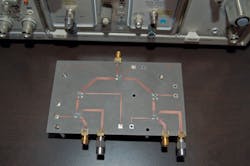
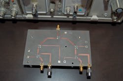
A prototype of the dual-channel switch circuit (Fig. 1) was constructed on 31-mil-thick RT/duroid® 5870 printed-circuit-board (PCB) material from Rogers Corp. It is a glass-microfiber-reinforced polytetrafluoroethylene (PTFE) composite material with dielectric constant of 2.33 in the z-axis at 10 GHz, and low dissipation factor of 0.012 in the z-axis at the same frequency. The RT/duroid 5870 board was reinforced for structural stability through the attachment of a 62-mil-thick FR-4 PCB to the back.
1. This is one possible circuit layout for the switch, fabricated on RT/duroid 5870 PCB material.
The switch improves upon switching circuit designs employing high-frequency relays. It offers increased bandwidth compared to a single-relay circuit, due to the use of microstrip distributed filters. These filters are fabricated in the form of tapered and nontapered microstrip transmission lines. The dual-relay switch achieves performance levels not possible in single-relay designs, such as the high isolation between channels, 50-Ω impedance at all ports with low VSWR regardless of the switch state, and low insertion loss across a wide operating bandwidth. The loop-through input port can be terminated into 50 Ω if not needed, or used as an additional input port that exhibits the full loss and isolation characteristics of the two main switch signal paths.
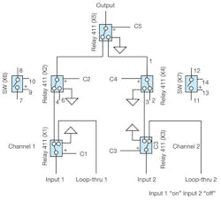
The switch circuit is configured as follows: Channel 1 consists of an input port (Input 1), an output port (Output), and a loop-through port (Loop-thru 1) which can connect to the input or output port. Channel 2 has its own input port (Input 2), the same output port (Output), and a loop-through port (Loop-thru 2) which can also connect to the input or output port. The loop-through inputs as inputs for additional switches or as additional inputs for a system using the dual-channel switch.
From Fig. 2, it may be seen that a total of five relays are used in the dual-channel switch, with relay X1 is connected to Input 1, Loop-thru 1, and relay X2. Relay X2 is also connected to relay X5, which is in turn is connected to the output port and relays X2 and X4. Relay X4 is connected to relays X3 and X5, while relay X3 is connected to Input 2, Loop-thru 2, and relay X4. Relay coils are connected to ground and to their respective control lines.
2. This schematic diagram shows the basic architecture of the loop-through switch.
The other contact points visible on Fig. 2 are the control-line connections: C1, C2, C3, C4, and C5. Control signals are DC voltages used to change the state of the applicable relay. For the relays used in the dual-channel switch, the control voltage is +5 VDC, although voltages of +6, +9, +12, +18, and +24 VDC can be used, depending upon the design of the relay coil.
When Input 1 is “on” and Input 2 is “off,” a signal at Input 1 passes through relay X1, relay X2, and output relay X5 on its way to the output port connector. The signal path at Input 2 is through relay X3 to the Loop-thru 2 output port. Relay X4 is switched “off” to prevent signal flowing from Input 2 and to increase the channel isolation.
When Input 2 is “on” and Input 1 is “off,” a signal at Input 2 passes through relay X3, relay X4, and output relay X5 on its way to the output port connector. The signal path at Input 1 is through relay X1 to the Loop-thru 1 output port. Relay X2 is switched off in this case to prevent signal flowing from Input 1 and to increase channel isolation. In the two-channel switch circuit, relays X2 and X4 are three-port components with an unused port for each. However, it is also possible to use two-port relays—say, X6 and X7—without the unused ports.
Unlike a traditional two-channel switch, Input 1 and Input 2 can both be switched “off” at the same time. When this is done, both input signals will be available at their respective loop-thru output ports, where they can be terminated in 50 Ω or used elsewhere in a system.
In evaluating the performance of the dual-channel switch, insertion loss (S21) was measured with all channel inputs terminated into 50 Ω and all loop-through outputs terminated into 50 Ω. The frequency response was measured as the ratio of the output voltage to the input voltage measured by the signal generator, with all switch ports terminated into 50 Ω. Isolation was measured as S21, with the input port switched off for each channel. This is the input to output port isolation, rather than the channel-to-channel isolation.
Return loss was measured with all channel inputs terminated into 50 Ω, the output port terminated into 50 Ω, and all loop-through outputs terminated into 50 Ω. The two-channel switch circuit was characterized with a commercial high-speed digital sampling oscilloscope (DSO), with model S-6 sampling head and model S-52 pulse generator head from Tektronix.
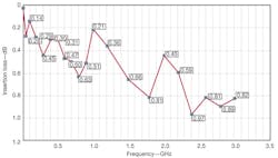
The broadband insertion loss (3-GHz scan) of the two-channel switch circuit was measured with the aid of a model HP 8664A synthesized signal generator from Hewlett-Packard Co. (now Agilent Technologies; www.agilent.com). Two measurements were made at each frequency: one with the 2 Channel Switch removed from the signal path, and the second with the 2 Channel Switch in the signal path. Using data from both results, the loss in dB was calculated. The plot shows a response of -0.05 to -0.97 dB over a frequency range of 10 MHz to 3 GHz (Fig. 3).
3. Insertion loss was evaluated through 3 GHz with level response across the full frequency range.
The return loss of the two-channel switch was measured with a model SP2369 autotester from Wiltron (now Anritsu) from 2 to 12 GHz. The VSWR across this frequency range is 2.0:1 or better whether the input port is active or not. Computer simulations of the switch circuit’s 11 behavior with the input port switch in the “off” position indicate that return loss is better than 40 dB at the lowest frequencies, rising to about 12 dB at 5.6 GHz.
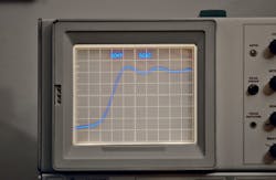
The risetime of the switch (Fig. 4) was determined by subtracting the risetime of the measurement system without the switch in place from the measured risetime of the same measurement system with the switch circuit under test. The formula is simply: [(measured risetime)2 – (system risetime)2]0.5 The system in this case is the S-52 pulse generator head, the S-6 sampling head, and the interconnect cables. This system exhibits a risetime of 37 ps. The measured risetime with the two-channel switch in place, as shown on the oscilloscope screen, is 60 ps. The square root of the sum of the squares of these two values yields a calculated risetime of 47 ps for the switch alone.
4. The two-channel switch circuit boasts excellent transient response, as shown by this oscilloscope display. The test signal source is a Tektronix S-52 pulse generator head with rise time of better than 25 ps, and the S-6 sampling head has a rise time of better than 30 ps.
In summary, by incorporating electromechanical relays and microstrip circuitry on a low-loss PCB material, it is possible to fabricate a five-port, two-channel switch with switched loop-through input ports. It features a bandwidth of DC to 5.5 GHz with low loss, high isolation, and excellent transient response, and maintains a characteristic impedance of 50 Ω whether a selected channel is in the “on” or “off” position.
Mark Scott Logue
19955 NW Pauline Dr., Portland, OR 97229; (503) 601-4358, e-mail: [email protected].
