Dive into EM/Circuit Co-Simulation of a T/R Front-End Module and Actively-Scanned Array, Part 2
Download this article in PDF format.
5G is poised to bring more integrated and sophisticated antenna and circuit modules to the modern defense and commercial electronics markets. Part one of this article examined today’s multi-technology circuit and electromagnetic (EM) simulation challenges and the software tools needed to support the successful design of 5G products.
Part two presents examples that illustrate the use of multi-technology in an EM simulation and EM/circuit co-simulation of an actively-scanned antenna array. Advanced technologies such as parameterized 3D cells, shape pre-processing and simplification, 3D EM extraction, and in-situ measurements are described.
Example: Multi-Technology RFIC/MMIC Package on Board
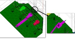
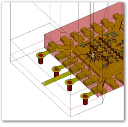
In this case, we’ll illustrate the use of multi-technology in an EM simulation. The area of interest is the launch from the board onto the package and then onto the chip within the package (Fig. 1). The board uses a printed-circuit-board (PCB) library. The device package utilized is quad, flat, no-leads (QFN).
1. Shown is an RFIC/MMIC in a QFN/flip-chip/wire-bonding package on a PCB.
The package is connected to the chip by means of bond wires. Three libraries are used in this example, one each for the board, package, and chip layout cells. The designer is interested in answering questions about the performance of the launch, grounding issues, package resonances, layout optimization, and performing yield analysis for manufacturability issues.
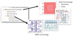
Hierarchy is being used in this EM project to control the multiple technologies. Each level uses one technology, ports and boundaries are added at the top level, and the final layout is then flattened and sent to the simulator (Fig. 2). Shown on the left is the list of layout cells. Notice the listing for “board partial package” at the top level, which uses a board technology. Also depicted is “full chip,” which is a sub-cell that leverages gallium-arsenide (GaAs) chip technology.
2. With hierarchy, each level uses one technology, ports and boundaries are added, and the final layout is flattened.
The NI AWR Design Environment employs the same stackup and material menus in each of the different technology libraries, making it easier to create and maintain the various technologies. In addition, different EM simulators use the same menus, enabling the designer to easily switch between EM simulators without worrying about different stackup or materials settings. For example, it is possible to switch between two different supported 3D simulators without any changes required other than for the simulator selection setting. Different simulators may implement the various settings differently, such as how they handle boundary conditions.
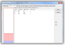
Figure 3 shows the stackup for a typical board. This same stackup can be used in AXIEM, Analyst, or third-party simulators without modification. The stackup also includes shape simplification rules, which simplify the geometry to produce a smaller mesh and reduce the problem size. The same simplification rules can be used for all simulators.
3. Each technology gets its information from the appropriate stackup block.
Ports and boundaries are placed at the top level of the layout. Note that a boundary for Analyst does not need to enclose an entire layout. Only EM effects inside the boundary will be simulated. Therefore, designers should be careful that important effects, such as coupling between the elements, are not left out when using this feature. The port type depends on the simulator. In Figure 4, Ports 1 and 2 are wave ports in Analyst, lumped ports in HFSS, and wave ports in CST, a Dassault Systèmes company.
4. Ports 1 and 2 are wave ports in Analyst and CST, but lumped ports in HFSS.
Parameterized 3D Cells
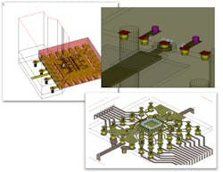
Libraries can contain 3D cells of pre-drawn shapes, which the designer can place in the layout. The cells can be parameterized, making it possible to modify the shapes by simply changing various parameter values—for example, the diameter or height of a BGA ball can be changed with parameters. These cells are sometimes called 3D parameterized cells (3D PCells). The layout in Figure 5 shows several 3D PCells being used, which in this case are bond wires and BGAs.
5. PCells can represent common types of 3D objects, such as bond wires, BGAs, QFN packages, and SMA connectors.
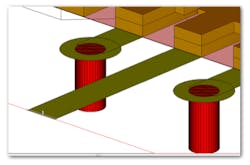
The grounding vias in Figure 6 represent another example of using 3D cells from the library. These vias were selected from the standard via parts list that ships with the library. The layout can be used for vias, multi-metal layer lines, and spirals. Fig. 6 shows the grounding vias from the board process design kit (PDK).
6. This figure illustrates grounding vias from the board PDK.
It is possible for designers to create their own cells by drawing them in the 3D layout editor integrated within Microwave Office. Parameters can be used in the drawing, which are then exposed in the software so that the layout can be easily changed. The custom cells can be added into the 3D parts library for use in other projects. In this way, companies are able to have their own proprietary parts libraries, which are shareable among all engineers.
Shape Pre-Processing and Simplification
Many features in EM layout are needed mechanically in the drawing, but are not necessary for the simulation. These features create many meshes when the problem is solved, which uses more memory and takes longer for the simulator to solve. Furthermore, very small meshes can be created, leading to a poorly conditioned problem and possible solver error.
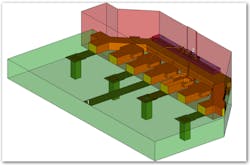
7. The board vias become squares after simplification rules have been applied.
The shape simplification technology in NI AWR Design Environment software is designed to solve this problem. PDKs have rules for shape simplification that remove small sides, unite vias, reduce the number of sides of circles/vias, and remove small indentations in multiple metal layers. Figure 7 illustrates how the board vias become squares after simplification rules have been applied.
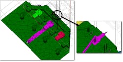
Simplification of the geometry, however, has its dangers. The various shapes may disconnect or nets can become shorted, although the engine tries to prevent this from happening. An annotation in the layout permits the designer to see the net connectivity after geometry simplification and meshing. Figure 8 is an example in which the various colors show the different dc connected nets.
8. Here’s a mesh example that shows connectivity.
Simulation Results
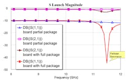
Figure 9 shows the results from simulating the package in Fig. 1. First, the front end only was simulated using the boundaries shown in Fig. 4. The boundary was then extended to include the entire package and subsequently the results were compared. The difference can be seen in the large dip in the magnitude of S11 due to a package resonance, indicating that the package needs better grounding.
9. Shown are the simulation results of the front end of the package along with the entire package from Fig. 5.
3D EM Extraction
EM extraction sends the layout of a schematic to the EM simulator automatically. This process usually involves a 2D layout that’s delivered to a planar simulator. Figure 10 shows an example of a MMIC spiral going to AXIEM. The picture on the left of Fig. 10 is a MMIC schematic with selected elements for extraction (highlighted in red), while the picture in the middle is the schematic layout. The picture on the right is the EM extracted layout in AXIEM.
10. In this example, a MMIC spiral is going to AXIEM for simulation.
Figure 11 shows an example of a module on a PCB going to AXIEM. Again, the picture on the left of Fig. 11 is the module schematic with selected elements for extraction. The picture in the middle is the schematic layout, while the picture on the right is the EM extracted layout.
11. Shown here is a module PCB going to AXIEM for simulation.
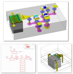
It is also possible to send a 3D EM extraction to a 3D simulator. Extracted shapes include thick, finite dielectric blocks, bond wires, boundaries, and ports. Figure 12 shows a 3D view of a MMIC module in which a MMIC chip is on top of a ceramic substrate with associated interconnects. In the top picture of Fig. 12, two different PDKs are used in the multi-technology example; the chip is attached to the substrate by bond wires. The picture at the bottom left shows the bond wires selected in the schematic, while the picture at the bottom right is the extracted transition in Analyst.
12. This figure depicts a MMIC multi-technology module in 3D (top) along with bond wires selected in the schematic (bottom left) and the extracted transition in Analyst (bottom right).
The straps from the ports to the bottom ground plane are used to obtain the correct port ground definitions. They are not made of metal; rather, they are mathematical surfaces used in exciting the meshes touching them.
Data Sets
Microwave Office uses data sets to help the designer manage the data from the various EM and circuit simulations. Data sets store simulation data, enabling designers to swap between data sets quickly to compare results on graphs and change the data used by a schematic (Fig. 13). Designers can take advantage of data sets to keep old simulation results and easily compare them with newer results. The data sets include the layout of the EM simulation and the log file.
13. Data sets in a project (left) can be easily plotted in multiples (right).
EM/Circuit Co-Simulation of an Actively-Scanned Antenna Array
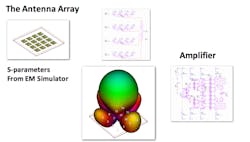
The antenna array and attached driving circuitry affect each other. To help designers overcome this issue, Microwave Office allows for co-simulation of the antenna and attached circuitry. First, the antennas must be simulated in an EM simulator, which produces an S-parameter file that describes the array’s behavior. Antenna patterns are also calculated from the known currents on the antennas. The problem is that the power amplifiers (PAs) driving the array are highly nonlinear and their performance depends on the loads they are driving (in this case, the inputs to the array).
14. This is an example of a 16-patch microstrip driven by 16 amplifiers.
As the beam of the array scans, the impedances of the ports change, which then affects the amplifiers. The antenna’s performance and the driving circuitry are therefore coupled together. Figure 14 shows a 16-patch microstrip example driven by 16 amplifiers. As the array is scanned, the load to each element changes, potentially degrading performance or changing power in some of the elements. This is not caused by the antennas; rather, it is because the load to the PAs has changed and must be accounted for.
In-Situ Measurement Feature
Traditionally, the designer must calculate the input impedance to the array, feed the results back into the circuit simulation, and then adjust the PA’s performance. The resulting output power is fed back into the array to see how the beam has changed. This cycle is repeated until the results converge—a time-consuming and painstaking process.
The in-situ (inside the circuitry) measurement feature in Microwave Office enables communication between the circuit and antenna, thus automatically accounting for the coupling between the circuit and the antenna array in an easy-to-use framework. The designer determines the measurement under consideration (such as the power radiated over scan angle) involving the circuitry that drives the various ports of the array by pointing to the S-parameter block on the circuit schematic.
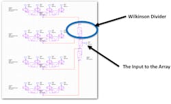
15. The corporate feed network is attached to the array in the circuit simulator.
The schematic in Figure 15 shows the corporate feed network attached to a 16-element array. The input to the array appears on the right side of the schematic. Wilkinson power dividers are used to split the power among the 16 elements (the blue circle indicates one of the Wilkinson dividers).
Before the signal reaches each of the 16 elements, it is sent through a transmit module. Each transmit module contains a phase shifter, an attenuator, and a PA. Figure 16 shows one of the transmit modules with the phase shifter, attenuator, and amplifier inside. The amplifier is driving the element and the array’s beam is steered by changing the attenuation and phase shift of each signal going into the antenna elements.
16. The MMIC amplifier is inside this transmit module.
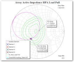
Because the PA is nonlinear, obtaining the correct performance requires accounting for the changing load in the PA as the attenuation is changed. Figure 17 shows the input impedance of an isolated patch element from 6 to 14 GHz (purple circle), as well as load-pull curves (green) for the amplifier and power output for various loads. As the antenna is scanned, the point on load-pull curves will change and the designer can account for those changes. In this example, the impedances of the array’s elements are about the same as the isolated patch, which meets expectations.
17. Shown is the input impedance of an isolated patch element from 6 to 14 GHz (purple circle), as well as load-pull curves (green) for the amplifier and power output for various loads.
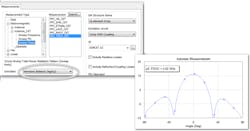
The pattern measurement is set up the same way. Since the power going to the elements is known, harmonic balance can be used for the circuit simulation in Microwave Office. Figure 18 shows the measurement of the total radiated power in Theta direction.
18. Harmonic balance is used for the circuit simulation.
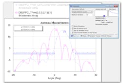
The pattern can then be optimized. In this case, the pattern is optimized by changing the phasing and attenuation to the array elements (Fig. 19). The purple pattern in Fig. 19 indicates the broadside excitation, while the blue pattern represents optimized performance, i.e., the side lobes are below the blue bars. The PA performance can be adjusted with the optimization.
19. The pattern is optimized by changing the phasing and attenuation.
Conclusion
Complex 5G and radar infrastructure requires the integration of antennas and circuitry. The challenge for EDA software is to support multiple technologies that require different circuit and EM simulators. Hierarchy at both the circuit simulation and EM level can be used to control multi-technology designs. And in-situ simulation is able to model antenna and circuit interactions.
Here's a video from EDI CON 2017 demonstrating EM/circuit co-simulation within NI AWR Design Environment:
Reference:
"IBM and Ericsson Announce 5G mmWave Phased Array Antenna Module," Microwave Journal
