Foundry Forms ICs for Space
Northrop Grumman is considered a designer and developer of major electronic systems for aerospace and defense applications. But supporting those major systems is a surprising semiconductor foundry capability such as the firm’s Space Park foundry in Redondo Beach, Calif.
The foundry produces large quantities of reliable integrated circuits (ICs) for critical applications such as space and electronic-warfare (EW) systems working with III-V compound semiconductor materials like gallium arsenide (GaAs). The devices are fabricated and tested to withstand the most challenging operating environments, including the radiation and temperature extremes of satellite-communications (satcom) systems.
The foundry focuses on developing what it refers to as “golden” chips or semiconductor devices that will operate within the harsh conditions of outer space for more than a decade, with operating frequencies extending well into the mmWave range (30 to 300 GHz).
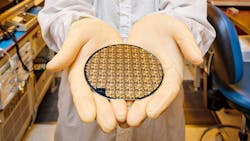
With recent supply-chain concerns over maintaining available semiconductors for space and other military and aerospace applications, the Space Park foundry is focused on producing large-capacity 4-in. wafers (see image above). It can also perform in-house, accelerated life testing, including thermal and electrical stress testing, thermal cycling, and hermeticity checks, to ensure that the semiconductors provide high performance levels over extended operating lifetimes.
In support of ongoing trends in military systems for reduced size, weight, and power (SWaP), the foundry creates ICs and wafers with increased density, with chiplets only 5 μm apart, and applies wafer-level packaging technology to hermetically seal semiconductor devices at the chip-scale level. These devices with increased density enable greater electronic functionality at smaller sizes and weights in support of longer-lasting satellites.
About the Author
Jack Browne
Technical Contributor
Jack Browne, Technical Contributor, has worked in technical publishing for over 30 years. He managed the content and production of three technical journals while at the American Institute of Physics, including Medical Physics and the Journal of Vacuum Science & Technology. He has been a Publisher and Editor for Penton Media, started the firm’s Wireless Symposium & Exhibition trade show in 1993, and currently serves as Technical Contributor for that company's Microwaves & RF magazine. Browne, who holds a BS in Mathematics from City College of New York and BA degrees in English and Philosophy from Fordham University, is a member of the IEEE.
