Novel Bonding Approach Helps Cool GaN Devices
Gallium nitride (GaN) is a wide-bandgap semiconductor material capable of high-power density and high-power levels at microwave frequencies. Because of the high power from such small transistors, thermal management has persisted as a challenge with GaN-based circuits, such as amplifiers.
Fortunately, researchers at the Georgia Institute of Technology have found a room-temperature means of bonding GaN to efficient thermally conducting materials such as diamond or silicon carbide (SiC) to draw heat away from the active devices. Such thermal bonds enable higher-power devices with improved reliability and reduced manufacturing costs for a wide range of RF/microwave applications, including wireless communications, radar and satellite systems.
The Georgia Tech researchers have designated the room-temperature approach as surface-activated bonding. It involves using an ion source in a high-vacuum environment to clean the surfaces of the materials to be bonded, such as GaN and diamond, to create dangling bonds on both surfaces. Small amounts of silicon are introduced into the ion beams to form strong atomic bonds between GaN and single-crystal diamond when fabricating high-power GaN semiconductor devices such as high-electron-mobility transistors (HEMTs).

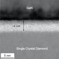
The new bonding technique yields a bond or interface region between the two materials that is only 2 nm thick, compared to about a 30-nm interface region using current higher-temperature bonding approaches in which diamond is integrated with GaN by nanocrystalline diamond growth. The thicker interface/bonding region effectively distances the diamond from the GaN, degrading the thermal conductivity path between the two materials.
Having a thinner bond region makes it possible to take full advantage of the excellent thermal conductivity of diamond and flow heat away from the source of the heat, the GaN substrate. By performing surface-activated bonding at room temperature, there is also much less thermal stress on the materials to be bonded compared to high-temperature approaches.
“This technique allows us to place high thermal conductivity materials much closer to the active device regions in gallium nitride,” said Samuel Graham, the Eugene C. Gwaltney Jr. School Chair and professor in Georgia Tech’s George W. Woodruff School of Mechanical Engineering. “The performance allows us to maximize the performance for gallium nitride on diamond systems. This will allow engineers to custom design future semiconductors for better multifunctional operation.”
The research was performed in collaboration with scientists from Meisei University and Waseda University in Japan and supported by a multidisciplinary university research initiative (MURI) project from the U.S. Office of Naval Research (ONR). For more on the current state of GaN semiconductor technology, don’t miss the feature story in the April 2020 issue of Microwaves & RF.
About the Author
Jack Browne
Technical Contributor
Jack Browne, Technical Contributor, has worked in technical publishing for over 30 years. He managed the content and production of three technical journals while at the American Institute of Physics, including Medical Physics and the Journal of Vacuum Science & Technology. He has been a Publisher and Editor for Penton Media, started the firm’s Wireless Symposium & Exhibition trade show in 1993, and currently serves as Technical Contributor for that company's Microwaves & RF magazine. Browne, who holds a BS in Mathematics from City College of New York and BA degrees in English and Philosophy from Fordham University, is a member of the IEEE.
