Microwave Transistor-Parameter Trade-offs in Circuit Design: Part 3
November, 1967
For a specific transistor process and family, a very strong relationship exists between the dc beta, hFE, and the high-frequency common-emitter current transfer ratio, hfe. This is primarily because of a basic difference between a high- and a low-beta transistor in a given process with fixed doping levels: The base width is narrower in a high-beta device; i.e., the emitter diffusion time is longer or the epitaxial thickness is less. A high-dc-beta device will also have a greater high-frequency current gain.
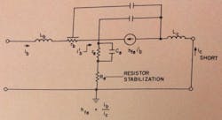
Fig. 1.Transistor-package circuit. This representation clearly shows that packaging has a significant effect on the performance of a transistor at microwave frequencies.
This file type includes high resolution graphics and schematics when applicapable.
The external hfe measurement is not necessarily the current gain of the internal device, since the measurement is made on the device in the package. A simplified model of the packaged transistor is shown in Fig. 1. Note that the capacitance distributed along the base resistance together with the other external capacitances will affect the short-circuit current gain of the device in the package. The package inductances and the resistance in the emitter structure will also affect the short-circuit current gain. Thus, the current gain of the package is not necessarily a good measure of the fT or hfe of the chip unless the reverse transfer admittance and other admittances are also measured and taken into account. This is an important consideration if the device is to be used for radiation resistance. Here a narrow base width is important rather than the effects of the package on the measurement of fT, which is used as an indication of base width.
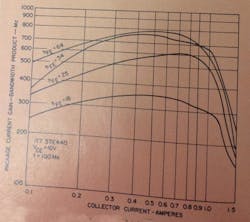
Fig. 2. Package gain-bandwidth vs collector current for various dc betas. A high-beta transistor with a low narrow base will exhibit current crowding at low current levels.
A high-beta transistor with a narrow base will exhibit current crowding at low current levels. The relationship between current gain-bandwidth product and collector current for different hFE levels (for a resistor-stabilized device) is shown in Fig. 2. The current gain of the packaged device is considerably less than the current gain of the device itself. This is because of degeneration cause by the resistance introduced into the emitter structure. At a current level of about 1.1 A a sharp dropoff exists in hf current gain (as was true of dc current gain) and this is a result of current crowding. The maximum current rating of a transistor is specified in an area where the hf and lf current gains are still useful. This explains the 1.5-A max collector current rating for this transistor.
To keep within the most linear portion of the transistor characteristics, the average current within the device should be held no greater than 1 A. It can be seen that a low-hfe device has less percentage change in hf current gain-bandwidth product than a high-hfe device. This is also true for hFE (or dc beta). The other variables which affect hfe are primarily resistors introduced into the emitter circuits of resistor-stabilized transistors, and current distribution for equivalent betas. The transistors represented in Fig. 2 have been chosen for equivalent emitter resistance to eliminate this effect on measurement. Other important correlations to hFE further validate the concept of what is happening in the base under the emitter.
Output admittance (yoe) to hFE relationship
This file type includes high resolution graphics and schematics when applicapable.
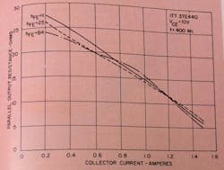
Generally, a high-hfe transistor and one of high-output capacitance have low real-output impedance. Actually, the output resistance at high frequencies in a small-signal analysis (simplified) approaches 1/(wtCo), where Co is nearly Cob. Thus, it is expected that where current crowding and current distribution have little effect, a high-dc-beta device will have the lowest output impedance. This is so in Fig. 3, where the parallel-output resistance is lower at low currents for a high-beta device than for one of low-beta. The difference, nevertheless, is rather small; and at high current levels, variations in distribution of the current and current pinch-off effect will probably mask this tendency as it does for these curves.
Fig. 3. Output impedance vs collector current curves show that the higher the dc beta the lower the output impedance, particularly at low values of collector current. The effect is not great, however.
It is important to note on these curves (which represent small-signal measurements of parallel output resistance) that output resistance decreases significantly as the collector current is increased. This provides a clue that the output resistance will be significantly lower in a large-signal circuit of an rf power amplifier than for the small-signal case or where the transistor drive level is low. Thus, the harder a transistor is driven, the lower the output impedance will become. Measurements of large-signal output impedance should bear this out. Output capacitance is fairly constant with current swing but not with voltage.
Collector breakdown-voltage differences will also affect the output impedance. For a single-type transistor, one with a higher BVCBO than another (and thus a higher resistivity) will have a lower output capacitance and subsequently a somewhat higher output impedance. The trade-off, however, is that the higher the collector-base breakdown voltage (and thus the resistivity of the silicon material) the lower the saturated power-output capability of the transistor. This condition increases the saturation voltage level and reduces efficiency as a transistor multiplier.
Input impedance (Zin) to hFE relationship
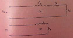
Fig. 4. Input circuit representations. Where the input capacitance is large, as for high-power transistors, the general circuit (a) can be simplified to that at (b).
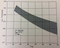
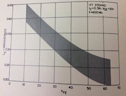
The input impedance of a transistor at high frequencies can be represented by the simple circuit in Fig. 4a. Assuming the input capacitance is large, as for a high-power rf transistor, the circuit can be reduced to that of a series inductance and a base resistance shown at b. The input capacitance decreases as the dc beta of the device is increased as shown in Fig. 5. Therefore, the hf input inductance becomes effectively smaller as the dc beta becomes greater. This is because the capacitive reactance will be larger and cancel out more of the package and circuit inductance. This is shown in Fig. 6 where the effective small-signal series inductance decreases as the dc beta increases. The large-signal value will also be different from the small-signal value. The inductance due to the package itself is of fixed value.
Fig. 5. Input capacitance vs dc beta. The capacitance decreases with increased beta, which means that the hf input inductance (Fig. 4b) becomes less as dc beta increases.
Fig. 6. Series input inductance vs dc beta (small signal). This phenomenon follows from the effect shown in Fig. 5 for input capacitance vs dc beta.
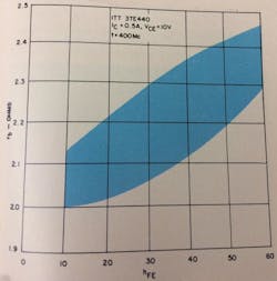
A high-dc-beta unit would be expected to have a higher base resistance since the lateral sheet resistance of the base under the emitter would be higher. The effect is fairly pronounced as shown in Fig. 7. The base resistance can increase by as much as 25 percent over the beta range of any transistor type. This is a small-signal base resistance and is lower in a large-signal condition.
Fig. 7. Base resistance vs dc beta. The lateral sheet resistance of the base under the emitter increases with dc beta.
Trade-offs
This file type includes high resolution graphics and schematics when applicapable.
From the curves it is assumed that a transistor with a high dc beta (and thus a high hFE) is relatively easy to match since it has a high input resistance and a low input inductance. But, matching is a significant problem because high-power, hf transistors have a large-signal real input impedance in the order of 0.2-0.7 ohm for a 20-50-W device. The trade-offs involved with high dc beta are:
- A high-beta transistor has greater tendency to oscillate and at lower frequencies.
- It is more difficult to maintain a constant bandwidth as a function of a circuit layout.
- It will have lower saturated-power output, although it will have higher power gain at most frequencies.
- It will be a less linear device and thus will have higher intermodulation distortion and less dc bias stability for single-sideband circuits.
Input-impedance to collector-current relationships
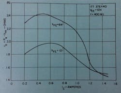
Fig. 8. Series base resistance vs input current. Note that lower dc-beta transistors have less variation in input resistance with current.
The input impedance should have less variation with collector current (or emitter current) if the device has a low dc beta. In Fig. 8 the series base resistance, rb, (or real part of h11e) has less variation with current for a low hFE transistor. A definite similarity of the impedance-vs-current curve to the hfe-vs-current curve exists. The same rapid change in resistance is observed in the same current region, as for dc beta and for hfe. It is also apparent from these curves that the large-signal impedance will be much lower than the small-signal value. This impedance in a tuned circuit is also affected by the stored charge and how the charge is drawn out of the device in the “off” part of the drive cycle. This would have the effect of lowering the input impedance still further. These curves show that the harder a transistor is driven (such that the average and peak currents become higher), the lower the input resistance. Large-signal impedance measurements show this to be true.
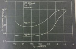
The series inductance, Ls, would also be expected to show variations with collector current, since the input capacitance changes with current. Typically, the input capacitance of a transistor increases as the collector current increases. The input capacitance would also be affected by the current pinch-off effect. Also, one would expect a more rapid input-capacitance change in the same areas where there are rapid changes in the input resistance, hFE, and hfe. Since capacitance increases with current level, the effective series inductance would be expected to increase likewise. This is because there will be less capacitive reactance to subtract from the package inductance. The theory is borne out in practice as shown in Fig. 9, where a larger change in input inductance occurs for a high-hFE device than one of low hFE. Both curves show a tendency to have rapid changes in series inductance above 1.1 A where this correlates with the same rapid changes in other parameters and in hFE itself. Inductance also increases with current. This corresponds with an increase in input capacitance with current. One must examine the combined effect of Ls and rb to see how the input circuit Q and package bandwidth are affected by current and hFE. Again, it should be noted that the large-signal input inductance will depend on the stored charge of the transistor and the class of operation. Thus, these curves can only give an indication of which way the values will go. Typically, the large-signal values of these curves will be somewhat different from the high-current values.
Fig. 9. Input inductive reactance vs collector current for low- and high-dc beta transistors. The low-beta transistor has less over-all reactance variation than the one with a high beta.
Package Q and sensitivity to series lead inductance
This file type includes high resolution graphics and schematics when applicapable.
Bandwidth capability of the transistor, and thus package Q, are an important consideration and not only for those applications where bandwidth is important. A low-Q input to a transistor (a low reactive part relative to the real part) is important for ease of matching to the transistor; it also improves circuit stability. The package input Q doesn’t determine the circuit bandwidth in itself. Other factors are the feedback effects of the load on the collector circuit and the degree of difficulty in matching to the low value of the input resistance. The higher the ratio of the source impedance to the real part of the transistor input impedance, the narrower the bandwidth; also, the more difficult it is to maintain the bandwidth when designing and cascading networks. A low package-input Q is of utmost importance as the first step in providing a good transistor for broadband applications and for ease in circuit design.
The circuit designer must connect the last element of the input matching network at some point external to the transistor package. This can’t be done without some finite package lead length and added inductance beyond what appears at the input to the package.
To maintain the low package Q, it is necessary to have a shunt capacitance to ground from the package input or from a point near it. Thus, it is quite important for good circuit design that the input-Q sensitivity to a change in the added series inductance external to the package be rather small. The small-signal bandwidth is:
The bandwidth sensitivity factor is defined as:
This sensitivity factor gives a relative measure of the bandwidth lost when a series inductance is added using the small-signal short-circuit impedance measurements as the criteria. It can only be a relative factor, because bandwidth is also significantly affected by changes in input impedance caused by the load on the collector.
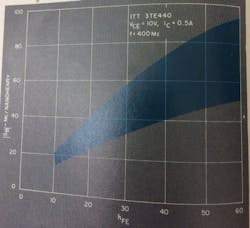
Fig. 10. Bandwidth sensitivity vs dc beta. One would choose a high-beta transistor for a high-input impedance for ease in matching and for lowest input Q.
Because the input impedance is a function of the transistor’s dc beta, it is possible to plot a range of values for the sensitivity factor SB vs hFE, using the measured values of the small-signal input parameters. This plot is shown in Fig. 10. Over the normal beta range for a given device type, the sensitivity factor can vary all the way from 15 Mc/nH to 90 Mc/nH at the high-beta end. There is a significant trade-off here. One would like to choose a high-beta device for a high-input impedance for ease of matching and for lowest input Q.
This creates a problem in that the bandwidth sensitivity is a maximum for a change in series inductance brought on by packaging or placement of components. A middle-of-the-road compromise is to choose a mid-range beta. More work will be required with actual broadband loads and large-signal input-impedance and bandwidth measurements to determine what the actual sensitivity factor is in a direct circuit operating mode. But the small-signal analysis indicates the direction of the tradeoffs. The small signal package Q is:
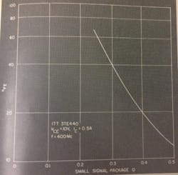
Package Q is dependent upon the hFE of the device. A typical median-range plot (Fig. 11) of many device measurements shows the approximate variation in package Q with hFE. Because of differences in resistor stabilization values, transistor resistivity, and uniformity of current and power distribution over the device, package Q can vary over quite a broad range either side of this median curve for a given hFE.
Fig. 11. How package Q varies with dc beta. Factors that affect this curve are resistor stabilization values, transistor resistivity and uniformity of current and power distribution over the device.
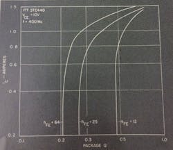
Fig. 12. Variation of package Q with collector current. Note rapid change in Q above the 1.1-A level.
Package Q is also a function of the collector current as shown in Fig. 12, and one would expect it to change even more rapidly as other parameters change at the same time.
Not the sharp change in package Q above the 1.1-A level for a 3TE440 transistor.
Large-signal input impedance measurements
This file type includes high resolution graphics and schematics when applicapable.
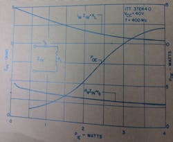
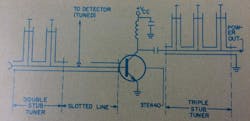
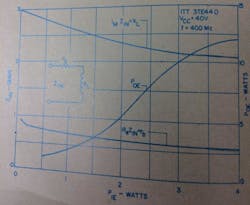
When one compares the small-signal data so far plotted with large-signal measurements in an operating circuit, good correlation is observed. A setup for a 400-Mc large-signal input-impedance measurement, with a tuned and matched collector circuit load, is shown in Fig. 13. Test results are shown in Fig. 14. The slope of the rb curve is sensitive to the heat sink employed. If a smaller heat sink were used, rb would increase with PIE. The large-signal rb, is seen to be lower in Fig. 14 than for the small-signal condition shown in Fig.14 than for the small-signal condition shown in Fig. 8 as would be expected. The input reactance is less than the small-signal value due primarily to the effects of the feedback from the collector load. But the package Q is 3.4 – much higher than the small-signal value.
Fig. 13. Large-signal input-impedance test setup for 400-Mc measurement. Test results are shown in Fig. 14.
Fig. 14. Large-signal input-impedance curves. Note that the large-signal rb shown here is considerably lower than for the small-signal case shown in Fig. 8.
Power gain as a function of transistor parameters
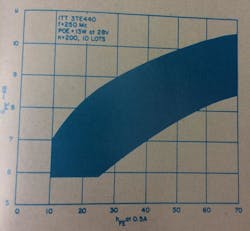
A significant trade-off between power gain and the other required transistor parameters exists for each particular circuit operation. Power gain is a function of frequency, and at high frequencies approximates 6 dB/octave roll off. The lower the frequency where a transistor is used, the greater the sensitivity of power gain to hFE. At quite low frequencies, as expected, power gain is controlled more by the hFE of a transistor than by other basic parameters. A 400-Mc transistor, for instance, demonstrates this phenomenon as shown in Fig. 15, when operating at the lower frequency of 250 Mc. A large lot sampling of the devices at this frequency gives the distribution shown. Obviously, low-beta transistors have significantly lower gain than those with high beta. The range is roughly from 6 to 10 dB for the normal hFE range of a device family. Thus, there is a significant trade-off between the power gain that can be expected and the other required device parameters which correlate to hFE.
Fig. 15. Power gain vs dc beta. At lower microwave frequencies, the power gain is controlled more by hFE than by other parameters.
In addition to correlation of power gain to hFE, it would also correlate to VCE(SAT). This is especially true where high VCE(SAT) devices are caused by either non-uniform current distribution or (for resistor stabilized devices) higher value resistors in the emitter.
Saturated power output trade-offs
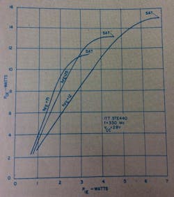
Saturated-power output capability is a significant and often overlooked characteristic of a power transistor. Among those presently marketed by many manufacturers, there is a wide range between the saturated-power-output capability and the specified power-output capability. Many designers tend to design around the saturated-power output if they can obtain this saturated power output without exceeding the dissipation limits of the transistor. In addition, the power a transistor dissipates under a high VSWR load condition is partially a function of saturated-power output capability. A significant trade-off exists between saturated power output capability and hFE. This is because of the current pinch-off effect under the emitter as previously described, where current peaks are more difficult to obtain with a high hFE.
Fig. 16. Gain saturation curves at 330 Mc. The lower dc beta transistors show significantly higher power gain.
Thus, device saturation would be expected at a lower level. Measurements of a device family, selected such that other parameters which affect saturated power output are equivalent in all devices at 330 Mc, are shown in Fig. 16. Here, a low hFE device has a significantly higher output level than one having high hFE. Also, note the differences in power gain as a function of hFE.
Another trade-off in the saturated-power output is with VCE(SAT). The higher the VSAT the lower the saturated-power output for a similar hFE. Table 1 shows roughly the trade-off between VCE(SAT) measured at dc and at saturated POE (the rf VSAT will be considerably higher but will also correlate). This is done on a high hFE unit to emphasize the correlation. A lower hFE device would not be quite as sensitive to the trade-off.
Table 1. Correlation of VCE(SAT) to POE(SAT) (For hFE = 60-65 units)
|
Unit |
VCE(SAT) (V) |
POE(SAT) (W) |
|
1 |
0.70 |
13.5 |
|
2 |
0.70 |
13.5 |
|
3 |
0.72 |
13.4 |
|
4 |
0.75 |
13 |
|
5 |
0.75 |
12.8 |
|
6 |
0.75 |
12.5 |
|
7 |
0.85 |
12.5 |
|
8 |
1.0 |
10.5 |
Saturated-power output would also correlate to the BVCEO transistor breakdown voltage because a high BVCEO would indicate a high resistivity collector. This, in turn, would indicate a higher VSAT or a lower saturated-power output. However, as previously noted, a high BVCEO unit would have less COB and more power gain. The trade-off between all of these parameters becomes somewhat complex.
Thermal effects, resistor stabilization and trade-offs
This file type includes high resolution graphics and schematics when applicapable.
The concept of resistor stabilization was introduced over two years ago for the express purpose of making a large-area hf silicon transistor operate uniformly and maintain a safe operating area. The concept that a high-power, hf transistor is nothing more than many small-signal transistors in parallel is a good premise to begin from. If this is true, and if differences exist in thermal dissipation of the device area plus differences in base width (and thus gain of some small transistors), a significant non-uniform distribution of current and power density over the large area of the high-power device exists. This is accentuated by the fact that a hf device has a high density of small transistors in parallel.
It is a well-known fact that if a bipolar transistor is heated up its gain will increase. Thus, the chip area that carries the most current will tend to heat up more than the surrounding areas and carry more of the load until it will blow itself out in that small area or “hot spot.” An obvious and direct method to equalize the current uniformity and power density is to put a small emitter resistor in series with each transistor. Such a large-area “resistor-stabilized” device operates more uniformly.
An increasing number of resistor-stabilized transistors are being introduced by semiconductor manufacturers. Thus, it is important to understand the trade-offs involved between resistor stabilization, thermal capability and operating characteristics of such devices. Since resistor stabilization is a form of emitter degeneration, power gain is degenerated as well. This is one of the more important trade-offs between thermal capability, safe-operating area and power gain. The higher the resistor stabilization, the lower the power gain. Thus, for a given power density and area, it sometimes is necessary to put a higher-gain device in for the same amount of resistor stabilization to maintain a useful over-all power gain. The more resistor stabilization is introduced, the higher the VCE(SAT) will be and the lower the saturated power output. This is a trade-off which is controlled by the manufacturer rather than the circuit designer, but it is an important one for the circuit designer to understand.
If device thermal resistances are compared, it is found that for a similar device type those with lower resistor stabilization will have a higher thermal resistance and less thermal dissipation capability. The significant trade-off here is one which relates power gain to saturated power output and VSWR capability (improved by resistor stabilization). Future devices will have improved forms of resistor stabilization structures built in, making these trade-offs less critical than at present.
Another plus feature of resistor stabilization is improved dc bias capability. This is combined with improved intermodulation distortion in single-sideband applications.
Thermal resistance and how to measure it
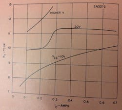
Contrary to the normal circuit-design concept, there is no such thing as a fixed thermal resistance for a transistor. Thermal resistance is normally defined as the temperature rise between the junction and the case per watt of dissipation. Because current uniformity (and thus power density) is a function of the current level as well as the collector supply voltage (or thus the power level in the transistor), one would expect thermal resistance to be a nonlinear function of these circuit parameters. Typically, current distribution is more uniform at low-current levels and is also more uniform at lower voltages. Thus, for a given transistor type, the low-voltage, low-current area will give the lowest value of thermal resistance. It is also to be expected that where one small area of the device tends to go into thermal runaway (i.e., has a negative slope of the base-emitter voltage vs collector current for a fixed collector voltage), that runaway will cause current from one area to suddenly shift to the area which is trying to carry more of the load. At this point, the active area of the transistor is effectively reduced resulting in high thermal resistance. This shows up as a sudden shift in a thermal resistance plot, as shown in Fig. 17. This plot of thermal resistance vs collector current as a function of dc collector-emitter voltage, is for a microwave transistor, type 2N3375. It substantiates that thermal resistance is a nonlinear function of these parameters, is much lower at low-current, low-voltage levels, and has discontinuities associated with sudden shifting of current and power density in the device. These effects, which are measured at dc, correlate reasonably well with the rf-power capabilities as well. Thus, it is important that the circuit designer be aware that thermal resistance is a function of the measurement conditions under which it is specified. Unfortunately, the conditions are very seldom specified on data sheet.
Fig. 17. How thermal resistance varies with collector current. The effect is nonlinear and much lower at low-current, low-voltage levels.
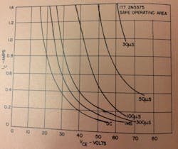
Because thermal resistance is a function of VCE and IC, it would be expected that the safe operating area under pulsed conditions would be a function of these parameters as well as the thermal time-constant of the device itself. If the safe-operating area under pulsed conditions is defined as that point at which some part of the junction area of the transistor reaches 200° C and pulsed measurements are then taken, safe operating curves are shown in Fig. 18, result.
Fig. 18. Safe-operating pulse conditions for a typical microwave transistor. These curves are based on the transistor junction area not exceeding 200° C.
VSWR capability, or the ability of a transistor to withstand a high VSWR load (i.e., approaching or equal to an open- or short-circuit condition) is an important consideration and correlates to some of the other transistor parameters. High-VSWR capability can relate closely to a transistor’s dissipation capability. Through part of the VSWR phase angle, the transistor must dissipate more power than in matched condition. Thus, a resistor-stabilized device, or one with a higher safe-operating area, can withstand this VSWR load better. The other trade-offs to obtain this capability are already apparent. Also, a device with a lower saturated-power output tends to limit its peak current more. Thus its total power dissipation is somewhat less. This is another direct trade-off between VSWR capability and the device itself. In the other phase of VSWR, a high-voltage, low-current condition exists on the collector. Here, a high-voltage break-down requirement and a sustained-high-current capability in avalanche are important. The trade-offs of high-voltage capability have already been discussed. However, high-avalanche sustaining-current capability has been difficult to relate directly to other basic device parameters that a circuit designer measures. It must be designed into the transistor.
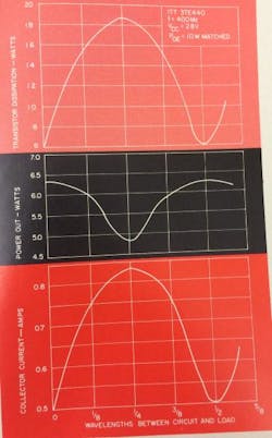
Fig. 19. Basic VSWR test circuit. Using this test setup one can measure the variation in transistor power dissipating, power output and collector current as a function of phase length between output circuit and load.
A typical variation in transistor power dissipation, power output, and collector current as a function of phase length between the transistor-output circuit and the load can be measured as shown in Fig. 19, with results as shown in Fig. 20 when adjusted for line losses. These curves illustrate how the phase between the output circuit and the VSWR load is important in determining what is happening at the transistor.
Fig. 20. Test results from setup of Fig. 19 show how the phase between output circuit and load is important in determining events at the transistor itself.
Summary
This file type includes high resolution graphics and schematics when applicapable.
It is important for the circuit designer to have a basic understanding of what is happening inside the semiconductor device to better understand its performance and the significance of circuit measurements. Much correlation exists between basic device parameters, which are easily measured prior to rf testing, and the characteristic performance of a device in its rf power-test circuit. With a reasonable knowledge of the basic relationships, the designer can estimate the performance of a given circuit for a distribution of device parameters. Much more work needs to be done to further characterize device parameters as related to circuit performance especially as it involves large-signal impedance measurements and hf breakdown characteristics as well as safe-operating area in an rf circuit. An attempt has been made in these three articles to show the relationships and trade-offs as they are understood today. The general ideas presented hold true for any device of the planar epitaxial type of construction regardless of the geometry or type.
References
Part 1:
John Tatum, “RF Large-Signal Transistor Power Amplifiers: Part I- Theoretical Considerations,” EDN, Cahners Publishing Co., (May, 1965).
Part 3:
E.O. Johnson, “Physical Limitations of Frequencies and Power Parameters of Transistors,” RCA Review, Vol. XXVI, No. 2, (June, 1965), pp. 163-173.
D.M. Smith and G.D. Vendelin, “High Frequency Silicon Power Transistors: Characteristics and Applications,” Texas Instruments Seminar Bulletin.
John Tatum, “RF Large-Signal Transistor Power Amplifiers: Parts I, II, III,” Electrical Design News, (May, June, and July, 1965).
John Tatum, “Circuit Improvements Utilizing the New Resistor Stabilized VHF Transistors,” Proceedings of the National Electronics Conference, Vol. XXI, (1965).
John Tatum, “UHF/SHF High Power Solid State Device Improvements,” Proceedings of the Southwestern IEEE Conference, (1965).
C.R. Turner, “Interpretation of Voltage Readings for Transistors,” RCA Application Note SM A-2, RCA Electronic Components and Devices.
H.E. Schauwecker, “Understanding Transistor Voltage Breakdown,” Electronic Design, (July 22, 1959), pp. 28-30.
