September, 1967
Aircraft radomes are traditionally considered to have only a mechanical function. However, consideration of dielectric-loaded slotted waveguide antennas suggests the possibility of incorporating such antennas directly into the radome. These antennas and the radomes commonly used in guided missiles are in fact highly compatible. For example, most of the dielectrics used in radomes are also used as substrates in flat, dielectric-loaded slot arrays. Moreover, the thickness of the material can be the same in both applications.
This article considers only low-loss plastic radomes. A conceptual radome-antenna incorporating several antennas is shown in Fig. 1. The array at the forward end has transverse slots; because of its position and end-fired radiation characteristics, its beam is directed along the longitudinal axis of the radome. The antenna located near the center section (four arrays, one in each quadrant) provides a complete conical beam around the body. A third antenna is a two-dimensional, planar, slotted array with a downward-looking beam normal to the radome axis. All antennas are flush-mounted and can be constructed as an integral part of the radome.
This file type includes high resolution graphics and schematics when applicapable.
Frequencies of the antennas described here are classified, but it can be stated that good results were obtained from L through C bands.
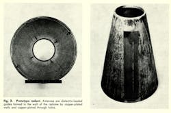
A composite radome-antenna (or radant) developed at Harry Diamond Laboratories is shown in Fig. 2. It is essentially a conical frustum made of silicone-fiberglass dielectric with dielectric-loaded slot antennas built into the surface of a 0.250-in.-thick radome. There are four antennas on the surface; each has five longitudinal shunt slots of varying length offset from the waveguide centerline. Each antenna is fed from a 50-ohm coaxial-to-waveguide transition. The top and bottom walls of the waveguide antennas are copper-plated. Waveguide edges are formed by plated-through holes closely spaced to minimize rf leakage.
The interior of the cone is completely copperplated, whereas the top slotted walls on the outside are plated in four places only. The plated interior minimizes rf energy within the radome. This model constitutes the basic, simplified version of an integrated radome-antenna system, a version that is relatively inexpensive to produce.
Antenna design principles
This file type includes high resolution graphics and schematics when applicapable.
The general concept, design parameters, and experimental techniques in developing dielectric-loaded antennas using flat, copper-clad, or copperplated dielectrics are discussed in Refs. 1, 2 and 3. These techniques are very useful in designing the basic antenna element for incorporation into the radome.
Keep in mind, however, that dielectric loading of a waveguide reduces its wavelength and phase velocity and also lowers the cutoff frequency. Thus, a smaller waveguide volume can transmit energy over a given frequency band, the cross-sectional area of a dielectric-loaded guide therefore is considerably smaller than the conventional air-filled guide for a given frequency.
Waveguides using solid dielectric as the propagating medium experience dielectric αd and copper αc losses in addition to the other transmission characteristics. These losses are small and sometimes can be neglected in waveguide antennas. But, at any rate, the losses are given by:
and
where
a and b = the waveguide dimensions,
ϵr = relative dielectric constant,
tan δ = loss tangent of the material,
fc = operating frequency.
Characteristics of longitudinal slots in dielectric-filled waveguides also are given in Ref. 3. Included are data on slot impedance and admittance as a function of slot length, as well as a discussion of slot scattering coefficients when the waveguide is excited in the TE10 dominant mode. The resonant length of a slot in dielectric-filled waveguide lies between half free-space wavelength and a half wavelength in the dielectric and is given by
where λ0 is the free-space wavelength.
Dielectric materials and plating techniques
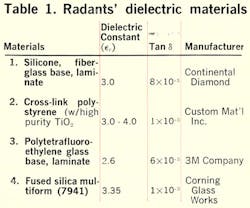
The radome material first used in our experiments was a glass-cloth laminate impregnated with silicone resin. A variety of other dielectric materials also have been copper-plated and used for dielectric-loaded slot antennas. Table 1 summarizes their electrical characteristics. Each material has some significant advantages. Important selection criteria are homogeneity, electrical characteristics, and behavior in a particular environment. Results of standard tests on these materials agree closely with data quoted by suppliers. Teflon-glass laminate and some of the silicone-based materials are particularly stable and well suited for waveguide fabrication. The adherence of the plated copper was very strong, and in most cases could withstand temperatures beyond 350° F without delamination. Metal is plated on the bare dielectric surface by an electroless process using no electrodes or electrical equipment. Objects of any desired shape or size can be plated. Surfaces are smooth and uniform without excess metal on the edges. Electrolytic plating is used thereafter to obtain desired metal thickness.
Slotted-array characteristics
This file type includes high resolution graphics and schematics when applicapable.
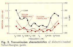
Two 12-in. sections of copper-plated waveguide (1/8-in. thick) terminated by 50-ohm coaxial connectors were built to determine operating transmission characteristics. Connectors were matched to the waveguide and positioned approximately λg/4 from the ends. One waveguide was built of silicone-fiberglass and the other of Teflon-fiberglass. Insertion loss in the Teflon-fiberglass section was slightly under 0.3 dB over a 300-Mc bandwidth, whereas that in the silicone-fiberglass was less than 0.5 dB over the same frequency range (see Fig 3). The input VSWR for the Teflon-fiberglass guide was less than 1.20 over a 400-Mc bandwidth and averaged about 1.10 between the limits of ±100 Mc from f0.
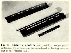
The center specimen in Fig. 4 is a bare silicone-fiberglass substrate section of one antenna array. The closely spaced holes forming the edges of the waveguide and the smooth surface finish are evident. The complete copper-plated array with radiating slots is also illustrated. In most cases only 0.003 to 0.005 in. of copper is plated on the surface. Note that the edges of the guide are cut along each side and through the center of the pleated holes; this was done to determine if any of the energy propagating in the waveguide radiated from the edges. Only a negligible amount of rf leakage was noted.
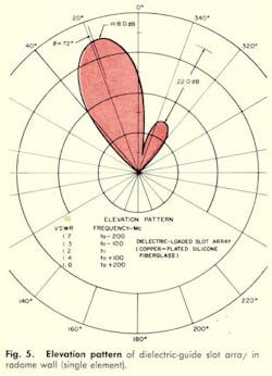
The array at the top of Fig. 4 is completely encased by copper-plating. Its radiation pattern is shown in Fig. 5.
Radant system performance
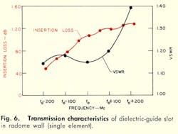
Insertion loss was measured of four waveguide test sections built into a radome before the slots were cut in the waveguide. The results (see Fig. 6) indicate insertion loss variation from 0.4 to 1.25 dB over a 400-Mc band. Normally, the insertion loss in a 12-in. length section averages 0.4 dB; however, because of the plated-through holes and epoxy coating used on the surface to minimize irregularities, as much as 1.25-dB loss was measured for the 14-in.-long section. With perfect samples and improved assembly techniques, the measurements over the same bandwidth indicated less than 1-dB loss. Insertion loss measurements taken on these antennas with the slots radiating varied from 8 to 12 dB. One-way elevation patterns of these antennas (measured in the radome) showed the average gain to be slightly above 7.0 dB with side lobes in each case suppressed 15 dB below the peak of the main lobe.
A two-way (two transmitting antennas, two receiving) azimuthal pattern taken on the antenna system is shown in Fig. 7. This is the radiation pattern generated around the body of the cone at an angle of peak intensity, or 72 degrees off the longitudinal centerline axis of the radome. The two transmitting antennas are diametrically opposite each other; the receiving antennas are positioned likewise. The peak gain of the (2 x 2) antenna arrangement as seen in Fig. 7 is approximately 9 dB. The symmetry is quite good, indicating good power balance in both the feed network and antennas.
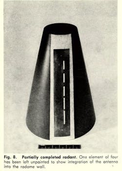
Figure 8 shows a partially completed radant. Three of the antennas are covered with a thin spray coat of epoxy-base paint. The fourth antenna remains exposed to illustrate the slotted antenna and part of the silicone plastic cone.
Other design approaches
This file type includes high resolution graphics and schematics when applicapable.
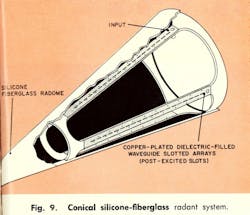
Because of some inherent difficulties in fabricating radants for certain special mechanical, environmental and electrical requirements—and the increasing interest in such systems, alternate designs were conceived. Extended development effort led to experimental prototypes shown in Fig. 9-11.
The silicone-fiberglass radome-antenna in Fig. 9 consists of a solid outer structure and a one-piece skeleton frame made of the same material. This frame is completely copper plated and includes four dielectric-loaded slot arrays. When the two sections are mated and properly secured with silicone resin, the over-all thickness of the radome is only 1/4-in. The assembly is sturdy and satisfies all mechanical requirements. This method of construction simplifies antenna design and fabrication; it also provides for improved antenna system performance.
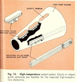
The radant of Fig. 10 was intended for short-time exposure to 2000-3000° F environments. The radome can be made from selected heat-shield materials. The three cavity antennas shown are copper-plated monolithic-dielectric structures. The basic antenna is a dielectric-loaded guide with a 50-ohm coaxial input which feeds a tee-bar coaxial-to-waveguide transition. Energy radiates through a thick window (approx. 1/2-in.) which is a party of the cavity. The dielectric is fused silica or other material compatible with the heat shield and the antenna. These antennas are characterized by their unusually small size and good efficiency in L and S bands.
An even smaller antenna that can be easily incorporated in high-temperature radomes is the copper-plated, dielectric-loaded ridge-guide antenna, also shown in Fig. 10. When used as illustrated, the array (0.625 x 1.25 x 10.0-in.) has a gain of approximately 5 dB at L band.
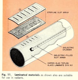
Figure 11 shows use of strip-line and dielectric-loaded slot arrays based on thing, copper-clad dielectric-laminates or printed-circuit boards.
Conclusions
Antenna systems designed as an integral part of a radome, fully utilizing the dielectric radome structure, clearly are feasible. The exploitation of dielectric-loaded waveguide techniques and the electroless copper-plating are instrumental to good performance and low-cost manufacture. Electrical performance is comparable to conventional systems and design techniques described should find widespread use in aircraft, spacecraft, and missile systems. Some of the more obvious advantages realized are:
- The incorporation of the antenna into the radome requires almost no additional space.
- The need for antennas inside the radome is eliminated.
- The design complexity is reduced.
- The rf leakage within the structure is minimized since the interior is completely copper-plated.
References
- “Slotted Antenna Arrays Can Be Smaller,” Howard S. Jones, Jr., Electronic Design, May 10, 1965.
- “Dielectric Loaded Waveguide Slot Arrays,” Howard S. Jones, Jr., TR-1269, Harry Diamond Laboratories, Jan. 22, 1965.
- “Radiating Slots on a Dielectric-Filled Waveguide,” Bernard R. Cheo, and Louis Pelish, TR400-118, Contract DA-49-186-AMC-183d, New York University, School of Engineering and Science, Aug. 1. 1965.
- “Plated Dielectric Waveguide Components,” Howard S. Jones, Jr., and R.J. Norris, MicroWaves, July, 1965.
- “Electroless Plating,” Product Engineering, p. 221, May, 1953.
