Optical Communications Inspired Amplifier Developments
OPTICAL TECHNOLOGY remains a critical aspect of today's communications infrastructure. Of course, it is now supplemented by myriad wireless technologies and services. While bandwidth issues were still being worked out with wireless standards, however, optical communications was pretty much the only solution for the high-speed-data demands of the Internet. As a result, the needs of optical networks drove the evolution of many components and technologies in the microwave industry. Transimpedance amplifiers (TIAs) were one such example.
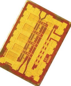
In an article titled, "TIAs Clear Way For 40-Gb/s Systems," a rundown of key TIAs were provided as well as an explanation of the technology evolution that they were enabling. The story, which appeared in the January 2002 issue (p. 33), emphasized that these amplifiers were going far beyond their traditional performance limits to provide the needed bandwidth. In fact, the TIA would become an even more crucial component as data rates moved to 10 Gb/s in Synchronous Optical Network (SONET) OC-192 and 40 Gb/s in OC-768 Ethernet applications.
The role of TIAs in these optical-communications systems is to boost low-level signals from a photodetector for further processing in an optical receiver. The TIA works directly with the output current from a photodetector (without a blocking capacitor). Often, the TIA also drives an automatic-gain-control (AGC) amplifier in these applications before signal regeneration. Among critical elements for TIAs in optical-communications systems is proper matching of the amplifier to the photodiode at 40 Gb/s. It also is essential to consider all of the characteristics of the TIA, photodiode, and other receiver components simultaneously. Special attention is paid to the control of the parasitic-circuit elements.
Due to the hot opportunity offered by the optical market's expansion, at least 24 companies had announced 10-Gb/s TIAs or planned to do so at the time of that article's writing. Among them were some that are still familiar and others that have been acquired or similarly disappeared: ANADIGICS, Philips Semiconductor, Vitesse Semiconductor, Velocium, Applied Micro Circuits, Maxim Integrated Products, Oki Electronic Components, Agere Systems, Intel, TriQuint Semiconductor, and Hitachi Semiconductors.
At the 10-Gb/s benchmark, most companies were using complementary metal-oxide semiconductor (CMOS), gallium-arsenide (GaAs), and silicon-germanium (SiGe) semiconductor compounds. Beyond 10 Gb/s, indium phosphide (InP) was eyed for a number of benefits. Companies that focused on the military and aerospace market, such as TRW and Raytheon, were pretty much the only ones with extensive InP expertise at that point. As a result, they were first to market with TIAs for these new optical-communications opportunities.
By using GaAs-based metamorphic-HEMT (MHEMT) technology, for example, Raytheon created a device that provided the high speed, low noise, and low power dissipation of InP-based HEMTs with the cost advantages of 4.0- and 6.0-in. GaAs wafers. Such hybrid approaches characterized the developments of this time, as they neutralized the fragility of InP and the lack of high-yielding, large-diameter substrates. This cutting-edge research and development brought the Internet to many homes across the country while laying the foundation for many of today's optical and semiconductor developments.
About the Author

Nancy Friedrich
RF Product Marketing Manager for Aerospace Defense, Keysight Technologies
Nancy Friedrich is RF Product Marketing Manager for Aerospace Defense at Keysight Technologies. Nancy Friedrich started a career in engineering media about two decades ago with a stint editing copy and writing news for Electronic Design. A few years later, she began writing full time as technology editor at Wireless Systems Design. In 2005, Nancy was named editor-in-chief of Microwaves & RF, a position she held (along with other positions as group content head) until 2018. Nancy then moved to a position at UBM, where she was editor-in-chief of Design News and content director for tradeshows including DesignCon, ESC, and the Smart Manufacturing shows.
