Transparentize Connections for 5G and WiGig Testing
Download this article in PDF format.
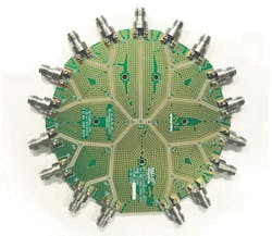
Critical to many new projects is a transparent interface to the board—one that you do not even notice is there. This connector-to-board interface is referred to as the board “launch,” where the RF energy transitions from the connector to the board. Figure 1 shows a typical design with 2.92-mm interface 40-GHz connectors on the edge of the board.
1. Shown is a 1:16 Wilkinson divider design that utilizes 2.92-mm connectors.
For designers moving to higher frequencies, i.e., into the 20-GHz range and higher, it will no longer suffice to just treat an SMA connector as a lumped 50-Ω element and mechanically join it to the printed-circuit board (PCB) using a standard footprint. For these designs, it’s now common to use 3D electromagnetic (EM) software tools, such as that supplied by COMSOL.
3D Tools Available to Designers
Designing a connector-to-board launch design is getting easier thanks to 3D EM software tools that have been available for years. Recently increased support from microwave connector suppliers is available as well.
Many microwave connector companies now provide 3D models of higher-frequency connectors that can be imported into 3D EM software tools. Some of these firms provide such models in a format that’s only compatible with a specific 3D EM software package. A fee may also be charged to receive the model. Signal Microwave models, on the other hand, are generic and can be used in any of the 3D EM software packages.
PCB material information is also available in many 3D solver packages. Signal Microwave goes beyond that by supplying reference designs for common high-frequency board materials. These reference designs, which are optimized by Signal Microwave, come in a common CAD format and can be imported into many 3D software tools. Customers are able to start with these reference designs and evaluate them using their own software tools. The design can then be used as is, or modified to better fit the customer’s requirements for final performance.
The Need for 3D Models
In 2D circuit simulators, the components on a PCB that operate at high frequencies can be modeled using S-parameters. This is not the case with a coaxial-connector-to-PCB transition. The transmission-line geometry in a connector is coaxial (circular). On a board, however, this geometry is planar. Correctly modeling how these two transmission-line types directly interact requires a 3D EM solver to address the complexities of the change in transmission-line mode from coaxial to planar.
Designs Start with the Board Material
Connectors are compatible with a wide range of board thicknesses and dielectric constants. The purpose of the board will determine the combination of board material, dielectric constant, and dielectric thickness requirements. The common board materials being used in the industry for high-frequency designs range in thicknesses from 4 mils (0.004 in.) to 12 mils (0.012 in.) with relative dielectric constants in the range of 3.0 to 3.5. Looking at these parameters, today’s high-frequency connector geometry matches up well.
Here is a quick checklist of required knowledge before starting the actual design:
- List of components and features on the board
- Determine line widths to match
- Determine loss and power requirements
- Choose a transmission-line structure
- Choose a suitable substrate
- Choose a suitable connector
Design Example
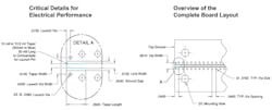
Figure 2 shows a 70-GHz bandwidth launch design of a grounded coplanar-waveguide (GCPW) transition between a Signal Microwave ELF67-001 connector and an 8-mil-thick Rogers RO4003 PCB.
2. Critical details of a 70-GHz bandwidth launch design are revealed in this design.
Key elements of the design include:
- Via size, placement, and spacing
- Circuit ground spacing to match the connector
- Signal-line width to create a 50-Ω transmission line
- Compensation of the signal line (taper) to account for the connector pin
How to Set Up the Simulation
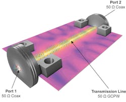
Figure 3 illustrates a short transmission-line structure with 3D models of the connector on either side. Signal Microwave supplies 3D models of the launch portion of its board-mount connectors. COMSOL Multiphysics software, a 3D modeling package, has many of these models in its library along with common board materials. Using such a structure, it’s easy to set up a two-port simulation model that can be used to optimize board designs.
3. This is a model of a transmission line structure with connectors, created using COMSOL Multiphysics software. (Courtesy of COMSOL)
Creating a through line with connectors on either end and creating the ports at the end of each connector simulation model will allow for the simulation of a structure that can be measured. The most efficient way to optimize the transition is by defining the ports as close as possible on either side of the section to be optimized. This would require creating a port in the transmission line of the board.
The domain between the inner and outer conductor of the edge-launch connector is filled with dielectric. Here, that dielectric is Neoflon, which has a dielectric constant of 2.5. All metal parts, including the edge-launch connectors, GCPW, metalized vias, and ground plane, are modeled as Perfect Electric Conductor (PEC) for low-frequency prototypes.
To consider loss factors and surface roughness at higher frequencies, the lossless PEC condition is replaced by Transition Boundary Condition and Impedance Boundary Condition. The entire modeling domain is defined by Scattering Boundary Condition, which represents an open space.
The physics-controlled mesh is chosen to get all domains meshed with a tetrahedral mesh; maximum element size is five elements per wavelength so that the wave is well-resolved. The maximum mesh size is automatically scaled by the material properties in the dielectric substrate. The parts in the edge-launch connectors are meshed manually with a finer resolution to provide good resolution of the curved surfaces.
Optimizing the Connector-to-PCB Transition
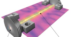
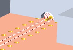
Energy flow from the coax to the PCB is represented in Figure 4. This simplified representation shows only the energy in the air portion of the transmission line. A significant amount of the energy is in the substrate and transitions from the dielectric of the connector to the substrate between the top and bottom conductors.
4. This figure illustrates the flow of energy from a connector to the printed-circuit board (PCB).
To fully capture the complexity of this transition at higher frequencies, a 3D simulation tool is required. Once the model is created and the ports are set to measure the energy flow (S-parameters), an optimization of the launch design can be done.
Sources of Discontinuity
The Pin Sitting on the Signal Line
The pin of the connector adds capacitance to the section of the board where it’s electrically connected (Fig. 4, again). This capacitance increases if the pin is soldered. Therefore, soldering is not recommended. The signal line of the PCB where the connector makes contact needs to be adjusted to reduce the effect of this extra capacitance (Fig. 2, again).
The Ground of the Connector Making Contact with the PCB
For a GCPW, the top ground spacing can be matched to the ground contact points of the connector. For a microstrip line, there’s no top ground. That means there is not much to optimize to improve performance. If a short GCPW section is added to the edge of a microstrip line, a structure is created that can be optimized to the connector.
The largest discontinuities occur at the section between the launch pin of the connector and the edge of the board. To simulate this, the TEM mode field is excited at the coaxial type lumped port, port 1. The field then propagates through the port 1 edge-launch connector and excites a planar mode on the GCPW. The symmetric electric field in the coplanar-waveguide is confined from the center conductor outwards to the conductors on each side and underneath. The listener port, port 2, is also terminated by the same type of coaxial lumped port.
The Need for a Trained Operator of the Software
The person running the simulation will need to know the basics of RF transmission lines. With this knowledge, one can properly oversee the implementation and then the results of the simulation. The software is able to quickly and easily explore a range of design features as defined by the user and provide data for each specific combination of features.
However, it cannot, for example, tell the user that a feature not in the design needs to be added, or that a feature in the design must be removed. These decisions have to be made by the user. The design can then be modified for further analysis through simulation. In this way, the software tool can be used to identify an optimized design and explore sensitivities in the design.
Sensitivity Analysis
The user will need to understand board-processing techniques and variances that are inherent in the board fabrication process. Understanding the strengths and weaknesses of holding tolerances in the fabrication process can guide users in the realm of sensitivity analysis. One should try to make the most difficult board-processing features the least sensitive in the design.
Conclusion
Projects will benefit from a well-designed board launch. Without efficient and well-behaved transition of energy into and out of a board, the performance of a board—or the components on a board—cannot be properly determined. In test, yield can increase when components do not fail due to degradation of test results that result from connector-to-board transition performance. In design verification, the accuracy of test results will improve as well.
High-performance board launches and transmission lines are achievable in projects in which their performance is critical. While not “transparent,” it’s close enough that the connector transition does not interfere with board measurements.
