Design High-Frequency Filters with Cross DGS Circuit Elements
Download this article as a .PDF
Lowpass filters can be designed and optimized by means of a new approach, based on the use of logarithmic series analysis and etched cross defected ground structure (DGS) topologies.1, 2
A simple J-inverter and coupling matrix enable the transformation of a lowpass filter (LPF) to a bandpass filter (BPF) with the same structure and conditions. In addition, Chebyshev guidelines, a suspended first-order layer technique, and logarithmic analysis are employed to design the filter’s operating frequency range. Lowpass filters were designed with cutoff frequencies of 2.0, 3.0, and 4.5 GHz, suitable for use in GSM900, radar, and wireless-local-area-network (WLAN) applications. The filters feature low insertion loss and high return loss in the passband, wide stopbands, and sharp rolloff characteristics.
Research on DGSs, such as photonic bandgap (PBG) transmission lines,3, 4 which have periodic arrays of defects, has been reported with various configurations in microwave and millimeter-wave frequency-band applications. A DGS with periodic or nonperiodic arrays provides a rejection band at some frequencies due to an increase in the effective inductance of the transmission line. The use of DGS technology has been reported for various applications, including filters,5-27 power dividers, and amplifiers, due to its high-quality-factor (high-Q) frequency characteristics, small size, precise equivalent circuit models, and simple implementation in microstrip circuits.
A conventional DGS consists of narrow and wide etched areas on a printed-circuit-board (PCB) material with backside metallic ground plane. The narrow and wide etched areas increase the effective capacitance and inductance, respectively, of a transmission line. A DGS is composed of two square defected areas and a narrow connecting slot, and these structures are the bases for the inductive-capacitive (LC) equivalent-circuit elements. An attenuation pole can be generated by the combination of the inductive and capacitive elements.
To explore the use of DGS circuit elements in high-frequency design, two different DGS LPFs and a DGS BPF were designed and fabricated. The second LPF design was extracted from the initial LPF using cascaded cross-DGS shapes and a J-inverter. Using Chebyshev’s rule and two additional cross-DGS elements, the third-order LPF was shifted from L-band to S-band. A logarithmic method was applied to improve the performance of the S-band fifth-order LPF. These DGS filters feature small size, low passband loss, and wide stopbands.
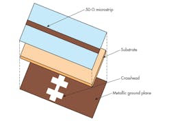
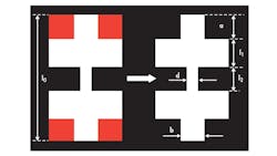
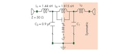
When a slot is etched in the backside metallic ground plane of a microstrip line, it disturbs the current distribution in the ground, and increases the effective inductance and capacitance of the microstrip line. Therefore, a DGS is usually modeled as a parallel LC resonant circuit by using a circuit-analysis method. Figures 1 and 2 show a DGS shape and its dimensions. Figure 3 shows an equivalent-circuit model, where L0 and C0 denote the inductance and capacitance, respectively, resulting from the current disturbances in the ground plane. For enhanced DGS modelling, circuit elements C1 and L1 were added to the equivalent-circuit model. The additional capacitance is from the fringing field around the discontinuity.
To extract equivalent-circuit-element values, the S-parameters of a DGS unit were calculating at the metallic ground plane using the Microwave Office EM simulator from AWR Corp. The relationship between these S-parameters and the ABCD matrix was used in designing the DGS filters. These simulations led to the following dimensions for the crosshead DGS section (Fig. 2): a = 2.8 mm; l0 = 15 mm; l1 = 2.7 mm; l2 = 3.85 mm; b = 1.8 mm; and d = 0.9 mm. The corresponding equivalent-circuit values for inductors L0, L1, and L2 and capacitors C0, C1, and C2, after using an optimization technique, were found to be L0 = 1.81 nH; L1 = 1.44 nH; L2 = 1.44 nH; C0 = 0.88 pF; C1 = 0.90 pF; and C2 = 0.90 pF.
Figure 4 provides a cross-sectional view of the proposed DGS section, located on the metal ground plane of a PCB. The crosshead slot exhibits an attenuation pole with a cutoff frequency without any periodic array of DGS circuit elements. Simulations of the cross slot with Microwave Office reveal one-pole LPF characteristics. Etching the slot in the metal ground plan increases the effective permittivity of the PCB structure, leading to an increase of the effective inductance of the microstrip line.
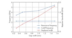
The dimensions of the crosshead slot determine the cutoff frequency. The etched gap, which connects both crossheads, has a significant effect on the resonance frequency, since it has inductive and capacitive characteristics. This explains the frequency characteristic of the proposed crosshead DGS. Figure 4 shows that by varying the gap width (d) of the DGS-resonator and keeping all other parameters constant, the resonance frequency shifts lower or higher in frequency depending of the variation. Increasing the canal width leads to a decrease in capacitance and an increase in resonance frequency, which is a shift towards the high frequency range (Fig. 4); a decrease in the canal width generates the opposite result.
Variation of the canal width also affects the width of the stopband of the DGS resonator. There is no change in the cutoff frequency despite the variation of the gap width.4 This means that the gap distance doesn’t affect the effective series inductance of microstrip. Variation of the effective capacitance only affects the attenuation pole position. As the etched gap distance increases, the effective capacitance decreases so that the attenuation pole position moves up to a higher frequency.
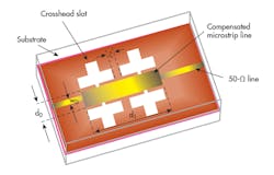
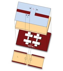
Figure 5 shows a schematic view of the cross-DGS LPF, composed of two uniform crosshead slots in the metallic ground plane of a microstrip circuit board and a compensating microstrip line on the top layer. Figure 6 provides the equivalent circuit. The three-pole LPF has dimensions of 30 × 20 mm2. The filter was fabricated on a circuit-board material with relative dielectric constant of 3.38 and thickness of 0.813 mm. The filter dimensions are as follow: w0 = 0.92 mm; d1 = 16 mm; d0 = 4.5 mm; and ξ = 2 mm. The remained dimensions are as noted earlier. The extracted capacitance and inductance values of the two DGS elements are: C0 =0.081 pF; L0 = 1.2521 nH; C1 = 0.036 pF; L1 = 1.307 nH; and C2 = 0.166 pF. The microstrip line on the top layer corresponds to a parallel capacitance.
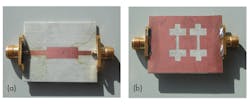
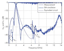
Photographs of the fabricated filter are shown in Fig. 7, while measurement results from a model HP8719D network analyzer from Hewlett-Packard Co. (now Keysight Technologies) are shown in Fig. 8. The measurements agree closely with EM simulations of performance. A transmission zero with about −33 dB rejection at 3.3 GHz is evident in the stopband of the LPF. These results indicate that this compact design (30 × 20 mm2) is advantageous compared to conventional DGS filters.5, 6 From the results, it can be seen that the LPF has better than 0.4 dB insertion loss from DC to 1.7 GHz with better than −35 dB return loss over the entire passband. Rejection is 30 dB from 2.6 to 14.0 GHz with very sharp transition from passband to stopband, from −1 dB to −35 dB within 1 GHz. As Fig. 8 reveals, this cross DGS LPF provides better performance than previous DGS LPF designs.5
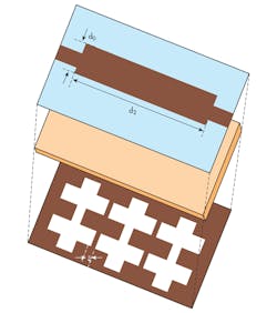
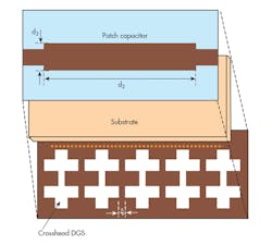
Figure 9 presents a diagram of the second cross-DGS LPF. It is composed of two uniform crosshead slots in the metal ground plane and a compensating microstrip line on the top layer of a PCB substrate. It was simulated as a three-pole LPF with crosshead DGSs on substrate with dimensions of 35 × 20 mm2. The substrate has relative dielectric constant of 3.38 and thickness of 0.813 mm. The new filter dimensions are d2 = 23 mm, with all other dimensions the same as for the first LPF design.
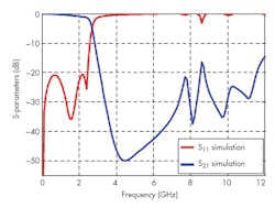
This second cross-DGS LPF features a simple design with low passband insertion loss of 0.85 dB and wide rejection bandwidth with 20-dB rejection from 3.2 to 11.5 GHz (Fig. 10). The compact lowpass structure occupies an area of 0.61λg × 0.35λg, where λg = 57 mm is the waveguide length at a cutoff frequency of 2.7 GHz. Such filter topologies are used in many communications systems because of their small size, low loss, and wide rejection bands.
Based on Chebyshev’s theorem, an LPF using five cascaded DGS resonators etched on the ground plane was designed and simulated. Neighboring cross-DGS elements are directly electromagnetically coupled to each other and indirectly electrically coupled with the microstrip feedline. The patch capacitor plays an important role in minimizing passband loss.
The filter is designed to operate at S-band frequencies. Increasing the number of resonators leads to an improvement of passband width, as well as an increase of the sharpness factor. Figure 11 provides a layout of the five cascaded resonators, while Fig. 12 shows that the S-band LPF measures 50 × 15 mm2 with relatively sharp transition band and good passband performance. It features wide rejection to 15 GHz and good harmonic suppression in the stopband. It was fabricated on RO4003 circuit material from Rogers Corp. and optimized with Microwave Office simulation software from AWR Corp.
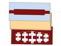
Based on the previous structure, the uniform distribution of five cross-DGS shapes was replaced by a nonuniform distribution (Fig. 13). The length of the cross shape was varied in proportion to the distribution of the relative amplitudes of the logarithmic function [ln(10)]1/n. For this method of logarithmic distribution, the length is defined as:
[ln(10)]1/n [ln(10)]1/(n-1) …[ln(10)]1/2[ln(10)]1[ln(10)]1/2 [ln(10)]1/(n-1) [ln(10)]1/n
For a conventional LPF designed with five cross-DGS resonators, n is the number of resonators minus 2, or the number of resonators divided by 2 and minus ½. In the current novel approach, n is equal to 3, and the relative amplitudes are calculated as follows:
[ln(10)]1/3 = 1.321;
[ln(10)]1/2 = 1.517;
[ln(10)]1 = 2.302;
[ln(10)]1/2 = 1.517; and
[ln(10)]1/3 = 1.321.
By comparing the corresponding ratios, the optimum lengths were calculated as follows: h2 = 8 mm; h1 = 10 mm; and h0 = 14 mm.
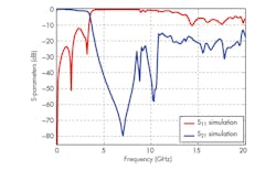
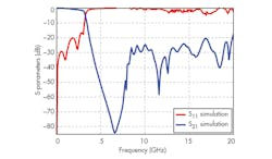
As Fig. 14 depicts, based on a previous filter structure with cascaded identical DGS resonators, a logarithmic method was used to improve the S-band LPF characteristics without a significant change in the previous topology. Compared to the previous fifth-order design, the proposed algorithmic structure has higher cutoff and resonance frequencies. As Fig. 14 shows, the proposed S-CDGS LPF topology offers low passband insertion loss and achieves a sharper cutoff and higher attenuation in the stopband compared to the previous fifth-order LPF designs. It provides a cutoff frequency and −20-dB stopband frequencies of 4 and 4.3 GHz, respectively.
The proposed filter achieves a broad −20-dB stopband from 4.3 to 20 GHz. The excellent sharpness factor and extended rejection band are due to the high characteristic impedance and slow-wave effect of a slot-back microstrip line. The cascaded DGS resonators of the lowpass structure were used to regenerate multiple transmission zeros (TZs) at 6.7, 11.5, and 13 GHz with attenuation levels of −32.81, −85, and −59 dB, respectively, and the wide stopband rejection, part of the spurious-free performance of the filter.
To understand the relationship between the scattering results and the energy flow along the proposed structure, it will be necessary to investigate the patterns of electric and magnetic energies along the cross-DGS structures. The field distribution of the S-band LPF continues until reaching the output (Fig. 13). At around 500 MHz, almost the entire magnetic energy is transferred from port 1 to port 2. The transmitted energy travels along the cross-DGS resonators and the 50-Ω microstrip lines, which serve as bridges to the output port.
The filter is in a passband state and the conductive metal area around the cross-DGS resonators exhibits inductive behavior (Fig. 15a). At 7 GHz, the total energy lies between the input port and the first cross-DGS resonator, so that the full input power remains focused within the first microstrip resonator and the excited feedline at the input port. This indicates that the structure is in a stopband state, undergoing a resonant effect at that frequency (Fig. 15b).
Design a Coupling Matrix
To realize a coupling matrix for an optimum filter structure, the desired specifications of the filter topology must be established. The required parameters can then be extracted using an optimization approach.28 The coupling coefficient and quality factor (Q) curves29, 30 will then be used to obtain the coupling coefficients. For the present case, the second-order filter has bandwidth (BW) of 1800 MHz, return loss (RL) of 20 dB, and center frequency (f0) of 4.3 GHz. The coupling matrix obtained from the optimization scheme is that of Eq. 1:
The external Qs are q1 = q2 = 0.711. To realize the normalized coupling matrix and Qs, a relationship of fractional bandwidth (FBW) to BW of FBW = BW/f0 was used, so that the actual (denormalized) coupling matrix becomes as shown in Eq. 2:
and Q1 = Q2 = Q = 1.693, where M = FBW × m, and Q = q/ FBW. The M-coupling coefficients and Q-quality factor will be inserted in the experimental curve28-30 to discover the optimal distance between the DGS resonators (ξ) and the shifting distance (d4) between the feed line and DGS resonator. The unknowns distances ξ and d4 are equal to 4 and 1.5 mm, respectively (Fig. 15). The extracted bandpass filter is designed to operate at 5.1 GHz for use in WLAN applications.
The structure has the same ground structure and size as the earlier L-band LPF design. On the top layer, there are two 50-Ω feedlines which are connected to the input and output ports via coaxial SMA connectors. Both microstrip lines are connected to each other via a J-inverter (Fig. 16), and thus electrically coupled via this gap (d4). The cross-DGS resonators are directly electromagnetically coupled and indirectly electrically coupled via RO4003 circuit material.
Because they are not close to each other, feed coupling can be neglected. Consequently, the mixed coupling created from both neighboring DGS structures is the only coupling that has an effect on the BPF performance. The proposed filter was designed, optimized, and simulated on RO4003 substrate and has a center frequency of 5.2 GHz for WLAN use.
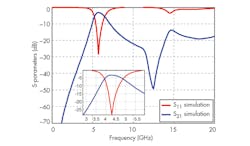
As Fig. 17 shows, the BPF topology has low passband insertion loss with wide upper stopband characteristic. The spurious suppression is better than −20 dBc for a frequency range which is more than 20 GHz. The simulated S11 return loss and S21 transmission loss of the BPF were −14.052 dB and 3.2361 dB, respectively. The upper −15-dB rejection band extends from 6.5 to 15 GHz. The lower −20-dB rejection band extends from 1.5 to 3.5 GHz.
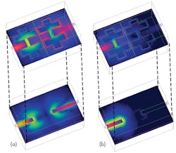
EM field distribution experiments were conducted on the bandpass filter at 1 and 4.3 GHz to better understand the effect of the C-DGS resonators on filter performance. Experimental results show that at around 7 GHz, a maximum amount of RF electrical energy is transferred from input to output using the J-inverter gap between both feed lines on the upper layer and both DGS resonators etched on the ground plane. The energy wave travels between the neighboring feed lines due to direct electrical coupling, while the transition between the feedlines and the DGS elements is due to indirect electromagnetic coupling. This indicates that the filter structure is in a passband state (Fig. 18a).
At 0.5 GHz, full RF input power is blocked between the input and the first cross-DGS resonator. Due to coupling via the printed-circuit structure, energy is transferred from the feed line to the nearest cross-DGS resonator. The energy oscillates between port 1, the microstrip feed, and the closest DGS-resonator but energy does not reach port 2, indicating that the filter structure is in a stopband state. As Fig. 18b shows, the filter structure undergoes a resonance effect.
Doctor-Researcher, Electrical Engineering
German Research Foundation DFG, Braunschweig-Bonn, Bonn, Germany
Doctor-Researcher, Communication Engineering, Telecommunications, Engineering, Electronic Engineering, University Sidi Mohamed Ben Abdellah, Fès, Morocco
References
1. S. Oh and Y. Kim, “A Compact Bandpass Filter Using Microstrip Slow-Wave Open-Loop Resonators with High Impedance Line,” Microwave and Optical Technology Letters, Vol. 38, No. 3, August 2003, pp. 185-187.
2. L. Liu, Y. Wei, X. Xu, F. Shen, G. Zhao, M. Huang, T. Tang, W.X. Wang, and Y. Gong, “A novel helical slow-wave structure for millimeter wave traveling wave tube,” proceedings of the 5th Global Symposium on Millimeter Waves Conference, 2012, pp. 312-315.
3. M. A. G. Laso, T. Lopetegi, M. J. Erro, D. Benito, M. J. Garde, and M. Sorolla, “Multiple-frequency-tuned photonic bandgap microstrip structures,” IEEE Microwave and Guided Wave Letters, October 2000, pp. 220-222.
4. Q. Xue, K.M. Shum, and C.H. Chan, “Novel 1-D microstrip PBG cells,” IEEE Microwave and Wireless Component Letters, Vol. 10, No. 10, October 2000, pp. 403-405.
5. “DGS Resonators Form Compact Filters,” Microwaves & RF, Vol. 5, May 2015, pp. 12-27.
6. “DGS and Multilayer Methods Make LPF,” Microwaves & RF, Vol. 3, March 2011, pp. 18-22.
7. A. Boutejdar, et al., “Compensating For DGS Filter Loss,” Microwaves & RF, February 2012, pp. 38-43.
8. A. Boutejdar, et al. “LPF Builds On Quasi-Yagi DGS,” Microwaves & RF, September 2013.
9. D. Ahn, J. Park, C. Kim, J. Kim, J. Park, Y. Qian, and T. Itoh, “A design of the low-pass filter using the novel microstrip defected ground structure,” IEEE Transactions on Microwave Theory
& Techniques, Vol. 49, January 2001, pp. 86-93.
10. L. Chiu, T. Yum, Q. Xue, and C. Chan, “A wideband compact parallel-strip 180° Wilkinson power divider for push-pull circuitries,” IEEE Microwave and Wireless Components Letters, Vol. 16, No. 1, January 2006, pp. 49-51.
11. David M. Pozar, Microwave Engineering, 4th ed., Wiley, New York, 2011.
12. A. Boutejdar, A. Elsherbini, and A.S. Omar, “A Compact Microstrip Multi-Layer Lowpass Filter Using Triangle Slots Etched in the Ground Plane,” Proceedings of the 36th European Microwave Conference 2006 (EuMC), Manchester, UK, September 2006.
13. A. Boutejdar, “Design of Compact Reconfigurable Broadband Band-Stop Filter Based on a Low-Pass Filter Using Half Circle DGS Resonator and Multi-Layer Technique,” Progress In Electromagnetics Research C, 2017, pp. 91-100.
14. J.-S. Lim, C.-S. Kim, Y.-T. Lee, D. Ahn, and Nam, “Design of lowpass filters using defected ground structure and compensated microstrip line,” Electronics Letters, Vol. 38, No. 22, October 2002, pp. 1,357- 1,358.
15. A. Boutejdar, N.M. Eltabit, A.A. Ibrahim, and E.P. Burte, “Design of Wide Stop Band L-Band LPF Based on DMS-DGS-Technique for Radar Applications,” Hindawi Publishing Corp. International Journal of Microwave Science and Technology, Article ID 101602, 2015, pp. 7-10.
16. A. Boutejdar, “Design of Compact Reconfigurable Broadband Band-Stop Filter Based on a Low-Pass Filter Using Half Circle DGS Resonator and Multi-Layer Technique,” Progress In Electromagnetics Research C, 2017, pp. 91-100.
17. Lin-Chuan Tsai and Ming-Lu Lee, “Design of Low-pass Filters Using Three-and Two-section Stubs,” Electron Devices and Solid-State Circuits, 2007 EDSSC IEEE Conference, December 20-22, 2007, conference proceedings, pp. 729-732.
18. C.S. Kim, J.S. Park, A. Dal, and J. Kim, “A novel 1-D periodic defected ground structure for planar circuits,” IEEE Microwave Guided Wave Letters, Vol. 10, April 2000.
19. A Boutejdar, “Design of a very compact HI-LO lowpass filter using meander technique and quasi horn inductors for L-band and C-band applications,” Microwave and Optical Technology Letters, Vol. 58, No 12, 2016, pp. 2,897-2,901.
20. L.-Y. Ren, “Quad-band bandpass filter based on dual-plane microstrip/DGS slot structure,” Electron Letters, Vol. 46, 2010, pp. 691-692.
21. A. Boutejdar, N.M. Eltabit, A.A. Ibrahim, E.P. Burte, and M.A. Abdalla, “New Compact Dual Bandpass Filter Using Coupled Double-Ring Resonators and DGS-Technique,” ACES Journal - The Applied Computational Electromagnetics, Vol. 31, 2016, pp. 132-137.
22. A. Boutejdar, A. Elsherbini, S. Amari, M. Awida, and A. Omar, “Design of a novel microstrip bandstop filter using one compact C-open-loop resonator,” in proceedings of the Asia-Pacific Microwave Conference, Yokohama, Japan, December 2006.
23. L. Liu, R. Jin, X. Bai, Y. Li, X. Liang, J. Geng, and C. He, “A tri-band bandstop filter with sharp rejection and controllable bandstop frequencies,” 2015 IEEE International Symposium on Antennas and Propagation & USNC/URSI National Radio Science Meeting, 2015, pp. 2543-2544.
24. A. Boutejdar, “A New approach to Design Compact Tunable BPF Starting from Simple LPF Topology Using a Single T-DGS-Resonator and Ceramic Capacitors,” Microwave and Optical Technology Letters, Vol. 58, 2016, pp. 1142-1148.
25. A. Boutejdar, “Entwurf, Entwicklung und Optimierung von kompakten HF-Mikrostreifen-Filtern mittels Defected Ground Structure-Technik (DGS),” Ph.D thesis, Otto-von-Guericke University, Magdeburg, Germany, November 2010.
26. M. Awida, A. Boutejdar, A. Safwat, H. El-Hannawy, and A. Omar, “Multi-Bandpass Filters Using Multi-Armed Split Ring Resonators with Direct Feed,” presented at the IEEE MTT-S International Microwave Symposium (IMS), Honolulu, HI, June 2007.
27. M.K. Khandelwal, B.K. Kanaujia, and S. Kumar, “Defected Ground Structure: Fundamentals, Analysis, and Applications in Modern Wireless Trends,” International Journal of Antennas and Propagation, Volume 2017, Article ID 2018527, 22 pp.
28. A. Boutejdar, A. Elsherbini, A. Balalem, J. Machac, and A. Omar, “Design of New DGS Hairpin Microstrip Bandpass Filter Using Coupling Matrix Method,” Progress In Electromagnetics Research Symposium, Prague, Czech Republic, August 2007, pp. 261-265.
29. M. Mokhtaari, J. Bornemann, and S. Amari, “Coupling-matrix design of dual/triple-band uni-planar filters,” in IEEE MTT-S International Microwave Symposium (IMS) Digest, San Francisco, CA, June 2006, pp. 515-518.
30. A. Boutejdar, “Design of 5 GHz-compact reconfigurable DGS-bandpass filter using varactor-diode device and coupling matrix technique,” Microwave and Optical Technology Letters, Vol. 58, 2016, pp. 304-309.

