Amplitude Equalizer Flattens Gain From 50 MHz To 7 GHz
This file type includes high resolution graphics and schematics when applicable.
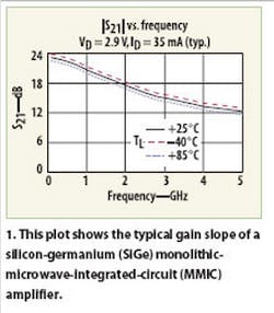
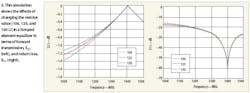
High-speed communications links are increasing the demand for wider link bandwidths. While many commercial companies are now offering monolithicmicrowave- integrated-circuit (MMIC) Darlington amplifiers internally matched to 50 Ω and designed to operate over multiple decades of bandwidth, these amplifiers have their limitations in terms of performance. While they are small in size and low in cost, one potential disadvantage is the gain slope that characterizes many of these amplifiers. Fortunately, developing a gain equalizer for these devices is generally a straightforward matter using lumped or distributed circuit approaches. While many manufacturers currently offer low-cost, broadband MMIC amplifiers for broadband-communications applications,1 these amplifiers can be plagued by a characteristic gain slope evidenced by decreasing gain with increasing frequency (Fig. 1).
Over a narrow frequency range, the gain slope can often be ignored. But for widerbandwidth use, it may require the additional of equalization. Fortunately, a simple lumped-element equalization circuit can be added that enables a much flatter gain-versus-frequency response to be achieved over a wide bandwidth using minimal components and printed- circuit-board (PCB) space. A distributed variant of the same equalizer topology can also be developed to extend its use to 8 GHz and beyond. Figure 2 shows a common equalizer topology.
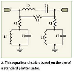
It is shown in pi attenuator form but can also be constructed in tee attenuator form.2 Its inductivecapacitive (L-C) component values are selected for resonance at some frequency just above the frequency band of interest. Far above and below this frequency, the circuit response is as a pi-attenuator. At resonance, the pi-attenuator is bypassed and the response exhibits zero loss (in theory). With the resonance set to just above the frequency band of interest, the circuit gives a positive gain-frequency slope that can theoretically counteract the negative gain slope of a typical broadband amplifier. This is achieved with excellent predicted return loss. The slope may be adjusted by either changing the LC values (maintaining the same resonance frequency) or by changing the piattenuator values. Unfortunately, this equalizer topology suffers from two major disadvantages at higher frequencies, namely, PCB layout parasitics and non-ideal lumpedelement performance. At 1 GHz, it has been the experience of this author that this circuit is extremely difficult to construct and could not be made to give the required positive gain-frequency slope. But, with some sacrifice in return loss, the simpler, more practical equalizer topology of Fig. 3 can provide realistic results.
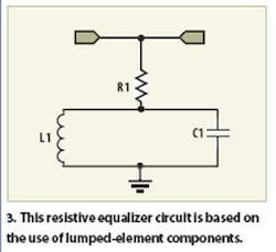
This provides a low component count, thereby reducing the effects of parasitic component pad capacitances and reducing the effects of non-ideal component properties. The equalizer essentially comprises a resistor in series with an LC resonator connected to ground. Again, the LC resonance is set to just above the frequency band of interest for the amplifier. The response well away from this resonance is governed by the resistor value and therefore higher values (typically greater than 110 Ω) are recommended to maintain a reasonable wideband return loss. The slope may be adjusted by varying the LC component values (maintaining a similar resonance frequency) or by changing the resistor value. This topology has been built, measured, and successfully used to cancel the gain slope of a commercial MMIC amplifier over a 250-MHz bandwidth.
For frequencies higher than 2 GHz, the inductor value required for an adequately high resonance frequency becomes impractically small. To avoid problems with circuit layout parasitics and poor lumped-element performance at frequencies above about 2 GHz, a distributed equalizer (Fig. 4) is preferred to the lumped-element version.
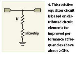
In place of the lumped LC resonant circuit (of Fig. 3), a printed resonator is used. The length of the resonator sets the resonance frequency and the width of the resonator sets the resonance quality factor (Q) and thereby the equalizer slope. The upper frequency limit of this topology may be limited by the resistor, in which case a substrate technology, such as low-temperature-cofired-ceramic (LTCC) technology, allows the use of a printed resistor. Care must also be taken where the microstrip resonator is grounded and provision for tuning the resonator length is recom-mended. Figure 5 shows the simulated ideal response of such a lumped-element equalizer circuit.
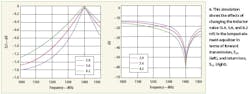
The S21 response of the lumped-element circuit is shown as the value of the resistor is changed. The capacitor and inductor values are fixed for a resonance close to 1.4 GHz and a positive gain-frequency response below 1.4 GHz. Lower resistance values result in more linear slopes over wider frequency ranges, at some sacrifice in wideband return loss. At frequencies away from resonance, the return loss is essentially the result of the selected resistor value in parallel with 50 Ω. Lower resistance values will yield degraded return-loss performance, and designers must decide whether the trade-off is acceptable. It is also of interest to examine how the equalizer response varies with resonance Q by changing the inductor and capacitor values while maintaining the resonance frequency at close to 1.4 GHz. Figure 6 shows that the linearity of the equalizer improves with lower Q values (higher inductor values).

However, higher Q values provide a steeper compensation slope, albeit over a narrower bandwidth. For more on predicting ideal amplitude equalizer performance, see the sidebar "Calculating Ideal Equalizer Performance." The ideal (theoretical) response shown in Fig. 6 suggests that the equalizer would provide a positive gain slope that could counteract the negative slope characteristic presented by the amplifier in Fig. 1 over a range of approximately 1.0 to 1.3 GHz.
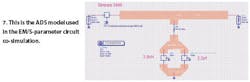
To investigate this with the help of computer-aided-engineering (CAE) software tools, a model of the lumped-element equalizer was constructed in the Agilent Advanced Design System (ADS)3 software suite by combining an actual layout simulation performed using the ADS planar electromagnetic (EM) simulator, Momentum, and device S-parameters from different manufacturers where available. As a result, the circuit co-simulation contains non-ideal elements, such as layout parasitic elements and inductor Q. This particular simulation contains S-parameters from Coilcraft (www.coilcraft.com) for the inductor, American Technical Ceramics5 (www.atcceramics.com) for the capacitor, and from Sirenza Microdevices (www.sirenza.com)1 for the amplifier. Figure 7 shows the Agilent ADS simulation file.
For this simulation, the capacitor value chosen was 2.2 pF, the inductor value chosen was 3.9 nH, and the resistor value chosen was 125 Ω. This gave a resonant frequency close to 1.4 GHz thereby providing amplitude equalization between 1 and 1.3 GHz. Figure 8 shows the performance of the equalizer circuit as predicted by the Agilent ADS simulation.
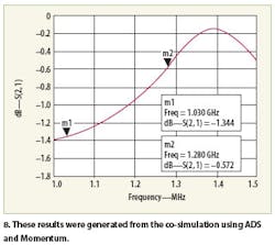
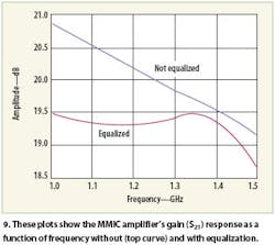
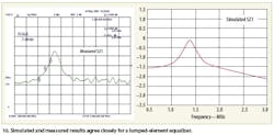
The gain is much flatter with the equalizer than without, with an equalized gain peak-to-peak variation of less than 0.2 dB from 1.00 to 1.34 GHz (a greater than 29-percent bandwidth). The Lband lumped equalizer described herein was constructed on an FR4 substrate and measured, with results close to predicted values. The amplitude equalizer topology described here may be implemented in either lumped or distributed form. The simplicity of the equalizer reduces circuit parasitics and allows operation to a higher frequency than more complex designs. A lumped-element version was simulated and shown to improve the response of an off-the-shelf MMIC amplifier (Fig. 10).
The author is working on distributed implementations operating up to 7 GHz.
References
- Sirenza Microdevices, model SGA3486(Z)_Datasheet.pdf, www.sirenza.com.
- Filter Equalizers, www.filtersolutions.com/passive.html.
- Agilent Technologies, www.eesof.tm.agilent.com/products/ads_main.html.
- Coilcraft, www.coilcraft.com.
- American Technical Ceramics, www.atcceramics.com.
This file type includes high resolution graphics and schematics when applicable.
