60- to 80-GHz LNA Boosts E-Band Radios
This file type includes high resolution graphics and schematics when applicable.
As wireless communications continuously push toward higher frequencies, bandwidth for radio waves that support high data rates has become available at millimeter-wave frequencies (above 30 GHz). Components are needed in support of communications systems at those frequencies, with one key component being the low-noise amplifier (LNA).
Among other functions, LNAs are vital for achieving high sensitivity and extended radio range in millimeter-wave receivers. With an eye to extending communications to frequencies at 60 to 80 GHz, an LNA based on graphene field-effect-transistor (GFET) active devices was designed and constructed for E-band radios. But, rather than use a traditional cascaded circuit stage, the amplifier employs current-reuse techniques, with a stagger tuning approach used to achieve wideband gain. Essentially, the LNA’s first stage reduces power dissipation through current reuse, while the second stage provides high gain via precision tuning for excellent output impedance matching.
In terms of active devices, FETs have seen wide use in high-frequency applications thanks to their quick responses to variations in gate voltage.1 This can be achieved by using a small gate length and high mobility of charge carriers.2 However, due to short-channel effects, FETs can suffer from drain-current saturation and drain-induced barrier lowering, as well as threshold-voltage rolloff issues.3,4 The impact of these effects on amplifier performance can be minimized by using an FET with a very small gate-controlled area.5
A Move to Graphene
Numerous semiconductor materials other than silicon have been utilized to implement millimeter-wave LNAs with high performance levels. These materials include graphene and compounds formed of Group III−V elements on the chemical periodic table of elements. Since graphene substrate material is composed of only a one-atom-thick, single layer of carbon atoms, it significantly reduces the channel area controlled by the transistor gate.
High-electron-mobility-transistor (HEMT) active devices based on Group III-V semiconductor materials have a channel thickness of 10 to 13 nm, which is greater than that of graphene-based FETs. Some silicon-on-insulator (SOI) FETs reported in the technical literature feature channel thickness of 2 nm, but they suffer low carrier mobility because of poor interfaces.6 These FETs are also characterized by variations in channel thickness, which result in fluctuations in device threshold voltage. This same problem occurs in HEMTs based on Group III−V materials if the channel thickness is reduced to 2 nm.7
To address these issues, research is being carried out on GFET-based devices for high-speed, high-frequency RF/microwave applications. Such research includes the design and development of a GFET-based LNA for millimeter-wave applications. In this LNA, a current-reuse stage is used for low power dissipation and to achieve high gain over a wide frequency range. It also includes a highpass inductive-capacitive (LC) filter to attain good input impedance matching. To improve noise performance, the amplifier incorporates an output buffer comprised of a source follower structure with no feedback.
Millimeter-Wave LNA Setup
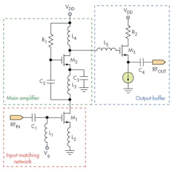
Figure 1 shows a schematic diagram of the millimeter-wave LNA. In the first stage, transistors M1 and M2 are mounted in a common-source configuration. An equal amount of bias current is shared between the two transistors to realize higher gain than an LNA in a conventional cascaded configuration. The source follower placed in the output stage acts as a buffer to achieve extended bandwidth by using the series LC resonance with the gate capacitance of transistor M3, Cgs3. The design of the millimeter-wave LNA can be detailed according to its three main sections: the input matching circuit, the main amplifier circuit, and the output buffer circuit.
While the LNA’s first stage is implemented with the function of reducing overall amplifier power consumption, the second stage’s design aims for good output impedance matching and achieving optimum amplifier gain across the frequency range of interest. The source of transistor M1 is connected via an inductor to stabilize the bias current. Coupling this source-degenerated inductor with the LNA’s integral highpass filter (HPF) produces input matching.
Since added resistance at this stage would increase noise figure for the overall circuit, the input impedance-matching network does not contain any resistors. As such, the source-degenerated inductor, L2, is used for input impedance-matching purposes. Using a T-equivalent model and the parasitic capacitance of the transistor eliminates the imaginary part for the impedance. Furthermore, the real part of the impedance is responsible for the 50-⦠impedance matching.
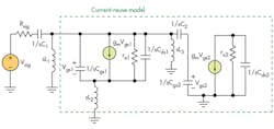
Figure 2 presents a simplified, low-frequency, small-signal, equivalent-circuit model of the impedance-matching network. The small-signal equivalent input impedance from transistor M1 to transistor M2 is calculated by using the following relationship for that impedance, designated as ZM12:
ZM12 = (ro1ÇÇ1/sCds1) + [(1/sCgs2 + 1/sC2ÇÇsL3] (1)
where the gate-to-source capacitance of transistor M2 is denoted by Cgs2. Inductor L3 and capacitor C2 are used for interstage impedance matching. Moreover, the output channel resistance of transistor M1 is ro1 and Cds1 is the capacitance between the source and drain of transistor M1. According to the resistance reflection rule, the input impedance Zinput can be written as:
Zinput = 1/sC1 + ({sL1ÇÇ(1/sCgs1 + [sL2ÇÇZM12/(1 + gM1ro1)]}) (2)
where L2 is the source degeneration inductor of transistor M1 and gM1 is the transconductance of transistor M1. The T-matching network is at the input of transistor M1, consisting of capacitor C1 and inductor L1. Capacitors C1 and Cgs1 form the imaginary part of the input impedance-matching network.
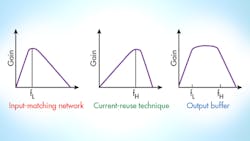
For lower power consumption, the LNA design employs a current-reuse configuration. The LNA makes use of two-stage cascade architecture for high gain and wide bandwidth. The first and second stages are designed to resonate at the lower and higher frequency bands of interest, respectively (Fig. 3).
Broadband operation is realized via a stagger tuning method, using the resonances of the two amplifier stages to achieve flat frequency response.8 The LNA’s first-stage lower resonant frequency, fLow, can be expressed as:
fLow = (1/2π)(1/L3C2) 0.5 (3)
The higher resonant frequency for the LNA’s second stage can be found from Eq. 4:
fHigh = (1/2π)(1/L4C4) 0.5 (4)
In this LNA design, the fLow and fHigh frequencies were chosen as 60 and 80 GHz, respectively.
The transfer of signal energy from the amplifier’s input to output ports for high gain is accomplished with the output buffer. This portion of the amplifier includes the output impedance-matching circuitry. Transistor M4 serves as the source follower. The low-frequency equivalent output impedance can be approximated by using the relationship of Eq. 5:
Rout = (1/gm3)(ÇÇro3ÇÇro4) (5)
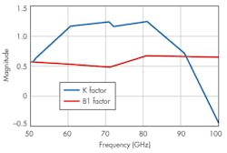
In general, if an LNA’s Rollett’s stability factor (or K factor) is greater than unity, the amplifier will be unconditionally stable over the full operating frequency range. Another parameter often used to evaluate the stability of an LNA is the B1 factor. If the B1 factor has a positive value, the LNA is said to be stable.
Performance Results
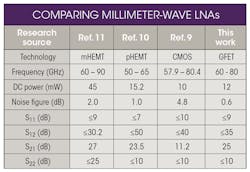
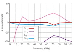
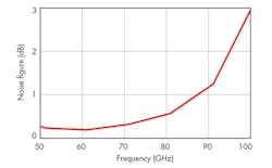
The millimeter-wave LNA circuit implements a GFET with channel length of 100 nm. The LNA’s power consumption was 12 mW with a +3-V dc supply voltage. The amplifier provides peak gain, S21, of 25 dB at 70 GHz. Across the full frequency range, peak gain is 25 dB and average gain is 18 dB (Fig. 4). Noise figure is less than 0.6 dB for the full operating frequency range of 60 to 80 GHz, which is a significant achievement at this E-band spectrum (Fig. 5). Also, K and B1 factor test results reveal high stability (Fig. 6). The amplifier achieves S11 of less than –9 dB, S22 of better than –10 dB, and S12 of better than –35 dB. The table offers a comparison of the millimeter-wave LNA’s performance parameters with a sampling of available state-of-the-art LNAs at these frequencies.
In short, this graphene-based LNA is a strong candidate for E-band wireless receivers and transceivers. The multistage design uses the same bias current for both common-gate and common-source stages, and features a cascode-based, current-reuse topology for low power consumption. Use of LC HPF circuitry accomplishes input matching and applying a stagger tuning technique achieves wideband gain. The GFET-based LNA shows significantly improved noise-figure performance compared to reported CMOS/HEMT LNA technologies (see the table) and may help to boost the development of radio receivers operating in the 60- to 80-GHz frequency range.
Yasir Sabir and Shabbir Majeed Chaudry are professors for the Department of Electrical Engineering at the University of Engineering and Technology, Taxila, Pakistan.
References:
1. M. Varonen, R. Reeves, P. Kangaslahti, L. Samoska, A.Akgiray, K. Cleary, R. Gawande, A. Fung, T. Gaier, S. Weinreb, A. Readhead, C. Lawrence, S. Sarkozy, and R. Lai, “A 75-116-GHz LNA with 23-K Noise Temperature at 108 GHz,” IEEE International Microwave Symposium Digest, Seattle, WA, June 2013.
2. You-Tang Lee, Chau-Ching Chiong, Dow-Chih Niu, and Huei Wang, “A high gain E-band MMIC LNA in GaAs 0.1-µm pHEMT process for radio astronomy applications,” 2014 44th European European Microwave Conference (EuMC), October 6-9, 2014, Symposium Digest, pp.1400-1403.
3. Yo-Sheng Lin, Chien-Chin Wang, Guan-Lin Lee, and Chih-Chung Chen, “A high-performance low-noise amplifier for 71–76, 76–77, and 77–81 GHz communication systems in 90-nm CMOS,” Microwave and Optical Technology Letters, Volume 56, No. 7, July 2014, pp. 1673–1680.
4. F. Schwierz, H. Wong, and J.J. Liou, Nanometer CMOS, Pan Stanford, 2010. ISBN: 9814241083.
5. D. J. Frank, Y. Taur, and H-S. P. Wong, “Generalized scale length for two-dimensional effects in MOSFETs,” IEEE Electronic Devices Letters, Vol. 19, July 1998, pp. 385-387.
6. I. Aberg and J. Hoyt, “Hole transport in ultra-thin body MOSFETs in strained-Si directly on insulator strained-Si thickness less than 5 nm,” IEEE Electronic Devices Letters, Vol. 26, September 2005, p. 661.
7. S. E. Thompson, R. S. Chau, T. Ghai, K. Mistry, and S. Tyagi, “In search of "forever continued transistor scaling one new material at a time,” IEEE Transactions of Semiconductor Manufacturing, Vol. 18, No. 26, June 2005, pp. 315-319.
8. Jaemin Shim, Taejun Yang, and Jichai Jeong, “Design of low power CMOS ultrawideband low noise amplifier using noise canceling technique,” Microelectronics Journal, Vol. 44, pp. 821-826.
9. Yo-Sheng Lin and Chien-Yo Lee, “9.99 mW 4.8 dB NF 57–81 GHz CMOS low-noise amplifier for 60 GHz WPAN system and 77 GHz automobile radar system,” Microwave & Optical Technology Letters, Vol. 57, January 2015, pp. 594–600.
10. N. Al Majid, S. Mazer, M. El Bekkali, and C. Algani, “Design of a V-band MMIC LNA for WPAN applications around 60 GHz,” 2014 14th Mediterranean Microwave Symposium (MMS), December 12-14, 2014, pp. 1-5.
11. P. M. Smith, M. Ashman, Xu Dong, Yang Xiaoping, C. Creamer, P. C. Chao, Kanin Chu, C. H. Duh, C. Koh, and J. Schellenberg, “A 50nm MHEMT millimeter-wave MMIC LNA with wideband noise and gain performance,” 2014 IEEE MTT-S International Microwave Symposium (IMS), June 1-6, 2014, pp. 1-4.
