What you’ll learn:
- Some brief theory and typical measurements of phase noise.
- How to produce the lowest phase noise at a PLL output.
- A standard design procedure for a typical Type 2, second-order loop.
As stated in Parts 1 and 2, phase-locked loops (PLLs) are ubiquitous in today’s high-tech world. Almost all commercial and military products employ them in their operation and phase (or PM) noise is a major concern. Frequency (or FM) noise is closely related (instantaneous frequency is the time derivative of phase) and is generally considered under the umbrella of phase noise (perhaps both might be considered “angle noise”). Amplitude (or AM) noise is another consideration.
While both affect PLL performance, amplitude noise is usually self-limiting and of no consequence. Phase noise, therefore, at the PLL output and of the RF components, is the dominant concern. Of course, output phase noise is the ultimate concern and depends critically on the phase noise of each component. A number of factors contribute to component phase noise, such as power supplies, EMI, and semiconductor anomalies, to name a few, and understanding these factors allows us to implement mitigation strategies for component phase noise and, ultimately, output phase noise.
In Part 3, we analyze our example hypothetical synthesizer to demonstrate the concepts and methods presented.
Example (from Part 2): Phase-Noise Analysis of 8- to 12-GHz Output/50-MHz Step PLL Frequency Synthesizer
We use our Phase Noise Analysis Procedure and Specific PLL Block Diagram & Phase Noise Propagation Model (Fig. 8, Part 2) for our analysis, which is done at five outputs: 8-9-10-11-12 GHz.
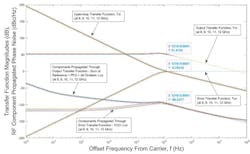
With all RF component phase-noise models previously developed using steps 1 through 6 of the procedure, we now use step 7 (see Part 2) and multiply all component phase-noise models by their applicable (output or error) transfer function magnitudes-squared to give their propagated phase-noise models. Along with the open-loop, output, and error transfer functions (discussed below), the models are simulated (Fig. 9).
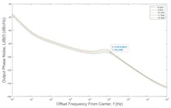
Then, we use step 8 of the procedure (see link above) and add all components’ propagated phase-noise models to give the output phase-noise model, which is simulated in Figure 10.
A. Open-loop transfer function, Tol (at 8-9-10-11-12 GHz outputs)
Referring to Figure 8, we have, from standard block diagram analysis, the open-loop transfer function, Tol (at 8-9-10-11-12 GHz outputs):
Simulate the five cases for TdBol(f) in Figure 9 (select Kϕ, Kv, N for 8-9-10-11-12 GHz outputs).
B. Components propagated through the output transfer function, Trc (at 8-9-10-11-12 GHz outputs)
Referring to Figure 8 again, we have the output transfer function, which is, again from standard block diagram analysis, an active lowpass filter, Trc (at 8-9-10-11-12 GHz outputs):
Simulate the five cases for TdBrc(f) in Figure 9 (select Kϕ, Kv, N for 8-9-10-11-12 GHz outputs).
Then, referring to Figure 8 once again, we apply our above analysis to the applicable components’ (reference, reference divider, feedback divider, prescaler, and phase detector) phase-noise models, represented by Lci. These are processed by Trc to find those components’ propagated phase-noise models, represented by Lco, which are simulated in Figure 9:1,4,5
Simulate the five cases for LdBco(f) in Figure 9 (select Kϕ, Kv, N for 8-9-10-11-12 GHz outputs).
C. Components propagated through the error transfer function, Tvc (at 8-9-10-11-12 GHz outputs)
Referring to Figure 8 yet once again, we have the error transfer function, which is, once again from standard block-diagram analysis, an active highpass filter, Tvc (at 8-9-10-11-12 GHz outputs):
Simulate the five cases for TdBvc(f) in Figure 9 (select Kf, Kv, N for 8-9-10-11-12 GHz outputs).
Then, referring to Figure 8 for the last time, we apply our above analysis to the single applicable component (VCO) phase-noise model, Lvi (scaled to 8-9-10-11-12 GHz from L11.3 at 11.3 GHz given on the datasheet). It’s processed by Tvc to find that component's propagated phase-noise model, Lvo, which is simulated in Figure 9:1,4,5
Simulate the five cases for LdBvo(f) in Figure 9 (select q, Kϕ, Kv, N for 8-9-10-11-12 GHz outputs).
D. Output phase noise (at 8-9-10-11-12 GHz outputs)
We now finish with our above analysis and add the components’ propagated phase-noise models processed by Trc, represented by Lco, and the single component propagated phase-noise model processed by Tvc, represented by Lvo. This will give the output phase-noise model, Lto, which is simulated in Figure 10:
Simulate the five cases for LdBto(f) in Figure 10 (select Kϕ, Kv, N for 8-9-10-11-12 GHz outputs).
So, the phase-noise analysis (modeling, simulation, and propagation) is complete and seems intuitively reasonable. Several things are evident from the simulation:
- The reference is clear in the close-in region from ~1 Hz to ~10 Hz with its first- and higher-order flicker contributions.
- The VCO is clear in the far-out region from ~100 kHz to >100 MHz, also with its first- and higher-order flicker contributions.
- The other components are clear in the mid-region from ~10 Hz to ~100 kHz with their floor (0th order) contributions and first-order flicker contributions.
This represents a fairly standard profile for most cases.
As mentioned previously, optimum phase noise is usually achieved by selecting the loop bandwidth at the intersection of the VCO and pedestal phase-noise curves for the mid-band output. However, in certain cases where it’s desirable to have more suppression of reference phase noise, the loop bandwidth can be made narrower to accomplish this with an attendant increase in VCO and floor noise. And, of course, if it’s desirable to have more suppression of VCO phase noise, the loop bandwidth can be made wider to accomplish this with an attendant increase in reference and floor noise. A tradeoff is always required.
Conclusion
We’ve shown how phase noise in general can be modeled and simulated, and how RF component phase noise propagates through a PLL to determine its output phase noise. We first discussed some brief theory and typical measurements of phase noise. We then discussed the analysis of phase noise and introduced our Phase Noise Analysis Procedure, which showed in detail the analysis method used by most CAD applications.
Finally, we demonstrated the concepts and methods presented by designing and analyzing a hypothetical single-loop 8- to 12-GHz output/50-MHz step integer PLL frequency synthesizer. It produced the lowest average output phase noise across the band by achieving the lowest phase noise at the 10-GHz mid-band output.
For our example synthesizer, we selected components and developed their phase-noise models (i.e., of the RF components). The component phase-noise models were then propagated through the synthesizer (i.e., the PLL) using their applicable transfer functions (output or error) to get their propagated phase-noise models. The component propagated phase-noise models were then summed together to give the output phase-noise model. All models were simulated to show their phase-noise curves. We did analyses at five outputs, 8-9-10-11-12 GHz, and the results seemed intuitively reasonable.
We also made use of MATLAB for its sophisticated computing power. Possible future endeavors might include a similar analysis considering more complex factors such as components with correlated phase noise and/or other subtle phenomena affecting output phase noise.
References
1. F. M. Gardner, "Phaselock Techniques", 3rd ed., John Wiley, Hoboken, NJ, 2005.
2. R. E. Best, "Phase-Locked Loops, Design, Simulation and Applications", 6th ed., McGraw-Hill, New York, NY, 2007.
3. P. V. Brennan, "Phase-Locked Loops: Principles and Practice", McGraw-Hill, New York, NY, 1996.
4. E. Drucker, "Phase Lock Loops and Frequency Synthesis for Wireless Engineers", 1997, Frequency Synthesis & Phase-Locked Loop Design, 3 Day Short Course, Besser Associates, Mountain View, CA, 1999.
5. F. C. Weist, "Phase Locked Loop Basics for Frequency Synthesizer Applications", Short Course, Clarksburg, MD, 2011.


