Members can download this article in PDF format.
What you’ll learn:
- Getting the most out of high-performance filters depends greatly on PCB design.
- Choices of board materials can greatly impact circuit performance.
- Grounding, plating, and metallization are important considerations.
As an RF circuit designer, you make many critical printed-circuit-board (PCB) design decisions to ensure your circuit will function as intended. These decisions range from selecting the right materials to developing a board configuration that will limit common issues, including spurious-wave-mode propagation, conductor and radiation losses, unwanted resonance, and dispersion.
However, as your circuit's operating frequencies rise into the mmWave range (30 to 300 GHz), the interactions of these short-wavelength signals with the board and its environment become intensified compared with signals in the microwave range (3 to 30 GHz). So, the challenges of board configuration and material selection become even more complex and important to the end-product's performance.
Because wavelengths at these mmWave frequencies range from 1 cm to 1 mm, the circuits require high-performance filtering. But if filters are to function optimally, you must be sure your PCB is configured appropriately. Just as a Maserati's performance would suffer from being driven with the tires you'd put on a lesser vehicle, your high-performance filters will not be at their best if you fail to optimize your board configuration.
In this article, we'll walk through a variety of board-design considerations for building circuits for mmWave applications. We also share some tips and tricks our engineers at Knowles Precision Devices have learned firsthand to help you get the most out of your high-performance mmWave filters in production.
Board-Configuration Techniques to Mitigate PCB Variation
PCB mounting and board-material selection are extremely important to achieving specified filter performance. Because there are too many board manufacturers to count, passive-component suppliers can’t possibly design board layouts that optimize component functionality for various frequencies on every board option. Therefore, each supplier usually includes a recommended PCB pattern to serve as a starting point.
When you begin a new circuit design, it’s important to know that this recommended PCB pattern may not be perfectly suited for your application’s needs, especially if you’re operating at mmWave frequencies. PCB land patterns will need to be optimized for different board materials and thicknesses to maintain the best voltage standing-wave ratio (VSWR) possible. Let’s look more in-depth at some of the different board-configuration considerations that can be tweaked to maximize performance at mmWave frequencies.
The Many Impacts of Board-Material Selection
To eliminate unwanted resonance and minimize wave-propagation issues, the selected board material should be thinner than one-quarter wavelength at the highest operating frequency in the given board material. Signal-conductor width will then be dictated by the thickness and dielectric constant (Dk) of the selected PCB material. In general, the thinner the PCB material, the narrower the required conductor width.
Since mmWave applications require thinner boards, etching tolerances must be extremely precise. Any variation in trace width or gaps in etching will have a greater effect on the system’s impedance, which will in turn degrade the VSWR. Also, due to the increasing need for more complex multilayer board construction that incorporates multiple plating steps, tightly controlling pattern definition on the outer layers of the board may be difficult to achieve because of the thicker copper cladding.
When thinking about board-material selection, it’s also important to note that the RF layer’s thickness and the Dk of the board material can increase or decrease the shunt capacitance that a device could encounter when fully mounted on the board. Therefore, to achieve the best performance, it’s important to optimize the board layout around and under the part.
Two additional, sometimes overlooked, material-selection factors that may impact the electrical properties of your board are moisture absorption and thermal properties. A good high-frequency material will have moisture absorption of < 0.3%. Regarding thermal properties, you should make sure the coefficient of thermal expansion (CTE) of the PCB material is close to the CTE of the ceramic components used on the board to avoid cracking.
Solder-Pattern and Reflow-Profile Considerations
Once the materials are selected and you start thinking about board assembly, one step that can greatly impact circuit performance, especially at mmWave, is the selected solder pattern and reflow profile. Let’s look at an example based on working with one of our devices.
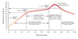
We recommend having a final solder standoff thickness of 2 to 3 mil once assembled. It should be used as a guideline to calculate the necessary solder apertures when considering your desired stencil thickness. This recommended solder-reflow profile has a maximum temperature of 250°C because devices with covers use a high-temperature solder, leaving the reflow at roughly 290°C. We don’t recommend that the reflow profile be much higher than 265°C. Figure 1 presents a visual representation of this example.
We understand that in some cases there may not be enough time or expertise for circuit board assembly companies to reliably place this recommended 2- to 3-mil solder thickness. Therefore, as an alternative, on-chip solder dams using dry film solder-mask material may be placed on the top of the circuit. If this needs to be done, just remember, solder masks typically have high moisture-absorption characteristics, which can cause a circuit material’s Dk to rise and losses to increase.
Grounding, Plating, and Metallization
To ensure high performance of your mmWave circuits, you also need proper grounding, plating, and metallization. First, ground-via spacing is important to consider at mmWave frequencies because higher-order modes can easily resonate between vias if spacing isn’t considered. To avoid this, a good rule of thumb for ground-via spacing is that the edge-to-edge spacing should be one-eighth of a wavelength or less at the highest operating frequency.
Next, multiple transitions between layers in a multilayer PCB will have a bigger impact on performance for mmWave applications. These transitions necessitate multiple plating steps that require thick copper to be deposited on the outer layers of the PCB. The tolerance of the thicker copper is much harder to control, which can be detrimental at mmWave frequencies as it will affect the VSWR.
In addition, the surface roughness of the copper cladding on the PCB will affect conductor loss much more at mmWave frequencies. While some board designers may want to use roughened copper to improve adhesion to the dielectric material and reduce cost, rougher surfaces essentially slow down a wave as it passes through the board. However, if differences in phase length or delays along a path will negatively impact an application, these factors must not be overlooked.
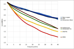
Furthermore, there are many possible plating finish options to consider as each option has its own advantages and disadvantages. Some of the most popular finishes available include electroless-nickel immersion gold (ENIG); electroless-nickel, electroless-palladium immersion gold (ENEPIG); and immersion silver.
When selecting a final plating finish, one important factor to consider is the insertion loss that the finish will add to your system. The plot in Figure 2 shows how different surface finishes can affect the insertion loss of a given transmission line on a PCB.
Transmission-Line Configuration Matters
While microstrip and grounded coplanar-waveguide (CPW) transmission lines can be used in these circuits, we recommend using a CPW versus a microstrip transmission line to improve isolation and reduce loss. When using a CPW, the electric-field concentration is greater in the air, producing less loss. On top of that, the ground reference is on the same plane with a CPW. Therefore, this arrangement improves isolation and creates less dispersion at higher frequencies.
Let Your Supplier Guide Your Decisions
When building a circuit for an application operating at mmWave frequencies, it’s likely you will need to deviate from the standard materials and thicknesses recommended for PCB assembly. To maximize performance, it’s a good idea to first discuss any potential board material or configuration changes, such as those covered in this article, and the effects of making these changes with your component manufacturer.
Most manufacturers, such as Knowles Precision Devices, want to ensure their filters function as intended. They are happy to work closely with circuit designers to walk through the nuances of building boards for optimal functionality at higher frequencies.


