Single-Ended GaN Power Transistors Spawn New System-Level Capabilities

Download this article in PDF format.
Equipment designers often face power-level requirements that far exceed what is achievable from a single solid-state device. While laterally diffused metal-oxide semiconductor (LDMOS) devices offer ever-higher power levels, gallium-nitride (GaN) technology takes it one step further: GaN brings higher power densities and efficiencies to the designer’s toolbox, making it possible to achieve even more power in smaller packages while reducing the overall size of the final solution.
Paralleling two or more RF power devices to increase power levels is still routinely done in the industry. However, a better way to scale power when combining multiple devices is to push the output power of single-ended transistors to significantly higher levels. This simplifies the bias needs and distribution, reduces size and weight, and enables additional system benefits previously contained in two rack-and-stack amplifier boxes. This article reports on the attributes and benefits of using these very-high-power transistors in the design and application of next-generation L-band systems.
Invigorating L-Band with GaN
As manufacturers address re-engineering existing L-band systems, GaN offers key benefits that lead to new capabilities. Bipolar transistors used in traditional avionics and radar capabilities have already been replaced by both LDMOS and GaN transistors to more than double power while maintaining power-supply dissipation levels. The new transistors’ greater levels of gain and efficiency are the main reasons behind the surge in power. Numerous suppliers already offer 500-, 600-, and 700-W transistors to make such a cascade possible. Figure 1 shows a conceptual block diagram of a typical 3.2-kW amplifier.
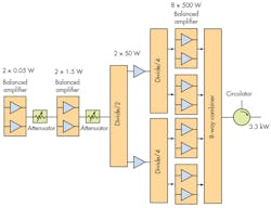
1. Shown is a block diagram of a 3.2-kW four-stage amplifier lineup at L-band.
A key driver of a high-reliability system design is redundancy. Thus, it is common to have parallel paths throughout the cascade chain, preventing soft failure. However, additional challenges arise in terms of bias distribution and the pulsing electrolytic cap placement.
GaN presents the additional challenge of introducing a negative supply voltage that also requires routing. To date, manufacturers have come to the system engineer’s aid by offering a wide array of balanced pallets with ever higher levels of integration. This has often been accomplished with what is called a “Gemini package”—two transistors and two leads at the input and output to allow for external combining (Fig. 2, left).
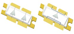
2. This image compares a high-power transistor in a Gemini package (left) with a single-ended 1600-W transistor (right).
Alternatively, a single-ended transistor can deliver the required higher power levels. One example is Microsemi’s 1011GN-1600VG 1600-W transistor, which is designed to combine higher RF output power with improved efficiency and ease-of-use in a smaller footprint.
The latest single-ended transistors combine multiple, large transistor cell arrays with high levels of efficiency while meeting all requirements for thermal performance and robust and reliable operation inside existing rack boxes. Figure 3 shows how combining two GaN-based, 1.6-kW, single-ended transistors can create upwards of 3 kW of power, simplifying dc and RF distribution and reducing the complexity, size, and weight of the final solution.
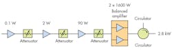
3. As seen in this block diagram, a 2.8-kW L-band amplifier utilizes a 1600-W single-ended transistor in a pallet configuration.
Size diminishes because the system engineer can use the two single-ended transistors to make two separate outputs available in an existing rack amplifier outline, eliminating one rack-and-stack amplifier (Fig. 4). That alone is a key step toward reducing overall system size and weight.
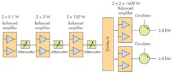
4. Shown is a block diagram of a dual-output, 2.8-kW L-band amplifier that incorporates four 1600-W transistors.
However, system size and weight shrink even more due to the small size of the single-ended transistor package—in the case of the Microsemi solution, just 0.385 × 1.340 in. (Fig. 5).
Within today’s small packages, the single-ended transistor application solution can include input and output matching circuitry as well as bias feeds. Special design techniques are used to minimize the size of the heat sink and metal pallet. This involves ensuring that output impedances have the ability to be set higher, so that the matching circuitry can be resized consistent with the transistor’s width.

5. The package size of this transistor is a mere 0.385 in. × 1.34 in.
At the same time, the use of impedance transformation techniques ensures the transistor can be shortened. In the case of the Microsemi devices, the application circuitry is created on 20-mil RO6010 material and measures less than 3.5 in. long by 2 in. wide (Fig. 6). This configuration also simplifies the bias scheme, which leads to fewer components and higher power gain and efficiency—even under Mode S-ELM signals.

6. This photo shows the application circuit of the 1600-W transistor.
GaN vs. LDMOS and GaN-on-Silicon
In addition to reductions in size, weight, and power, GaN-enabled transistors in a small, single-ended package outperform less-capable technologies such as LDMOS and GaN-on-silicon (both of which lack the necessary power densities, thermal performance, and efficiencies to address the next generation of avionics equipment).
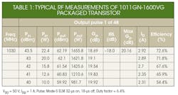
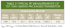
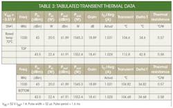
Tables 1 and 2 summarize the performance and efficiencies of designs using single-ended transistors. Drain efficiencies exceeding 70% make it possible to reduce device heating and allow the transistor to operate reliably under typical system environmental requirements. Tangible benefits go beyond higher power levels to include lower pulse droop—even in Mode-S applications.
This performance data is illustrated in Figure 7. The transistor demonstrates high levels of pulse-to-pulse stability, linearity, and droop.
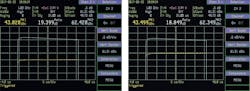
7. These screen captures depict performance at 1.03 GHz.
To maximize power performance, it is essential to maintain the highest efficiency. Thus, it becomes possible to maintain the lower operating channel temperatures essential for robust application reliability and satisfy the general lifetime requirements of high-reliability systems. Performance measurements consist of both average and transient thermal measurements using QFI (www.quantumfocus.com) thermal-imaging equipment, backed by thermal modeling and extraction of the true channel temperature (Fig. 8).

8. This test setup was configured to perform thermal measurements.
Single-ended transistors must demonstrate excellent balance on both the top and bottom transistor arrays inside the package (Figs. 9 and 10, and Table 3). In this example, the temperature difference is less than 5 degrees, demonstrating that each cell is being driven in amplitude and phase. As a result, high levels of combined efficiency and performance are achieved.
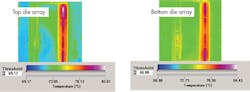
9. Shown here is average thermal imaging with these conditions: VDD = 52 V, pulse width = 32 µs, and pulse period = 1.6 ms (frequency = 960, 1090, 1215 MHz).
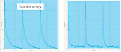
10. Illustrated is transient thermal imaging with these conditions: VDD = 52 V, pulse width = 32 µs, and pulse period = 1.6 ms (frequency = 960, 1090, 1215 MHz).
The benefits of GaN are well known, but only with the recent advent of single-ended GaN transistors has the technology emerged as a promising alternative to LDMOS—one that can dramatically reduce the size and weight of avionics systems. With the right combination of high power levels and over 70% drain efficiency, these devices will usher in new levels of system integration and power performance that was once only possible with bulky combinations of lower-power transistors. On top of that, they will maintain their efficiency while simplifying the overall application solution.

