Download this article in PDF format.
Evolving communication standards like LTE-A and 5G are driving future RF architectures and, consequently, creating challenges for RF front-end module design in terms of miniaturization, performance, and support for technologies that boost data throughputs by improving spectral efficiency.
To meet the ongoing need for higher performance and reduced component size in multimode- and multiband-capable handsets, companies are shifting their module integration strategies from combining similar building blocks in a single package to adopting multifunctional front ends based on diverse technologies. These development efforts target products based on a single, fully integrated RF module for each frequency range, including multimode/multiband power amplifiers (PAs), duplexers, RF switches, and RF matching.
Module and subsystem designers often use more than one technology in a complete design. These technologies include gallium-arsenide (GaAs) and gallium-nitride (GaN) monolithic microwave integrated circuits (MMICs), silicon (Si) RF integrated circuits (RFICs), and multiple-layer laminates. Each technology is encapsulated in a specific process design kit (PDK) that details the electrical and physical attributes of the manufacturing process and front-end building blocks (component libraries).
A multi-technology design flow that supports multiple PDKs and circuit/electromagnetic (EM) co-simulation is used to analyze the electrical interactions between the bulk-acoustic-wave (BAW) and surface-acoustic-wave (SAW) filters (based on equivalent circuit models) and multi-layer laminate package. It provides comprehensive module analysis and optimization. However, the Si RFIC switch, low-noise amplifier (LNA), and PA development is often executed in Cadence software using a Cadence Si PDK.
This article presents a modern design flow that translates the Cadence PDK into one that can be simulated in the NI AWR Design Environment platform to support chip-package co-design and EM verification. By importing the design into a dynamic library that can be used alongside the Cadence PDK, designers are able to effectively develop products based on disparate technologies using complex designs originally created in completely different environments.
EDA Tools are Built for Specific Needs
Designers use different RF electronic-design-automation (EDA) tools based on personal preference and the capabilities of a particular tool to address a single or set of design tasks. Some tools specialize in high-frequency MMIC, printed-circuit-board (PCB), and module design, such as Microwave Office circuit design software. Others like Cadence target silicon-based RFIC and module design. Since each of these tools have their own individual strengths, it’s best to adopt those that support interoperability and the exchange of information in a well-defined design flow so that designers can take advantage of the best tool for each design task.
To support data exchange between different environments, several industry-standard file formats have been developed, such as touchstone (SNP) and measurement data interchange format (MDIF) files. The touchstone file provides S-parameters, the small-signal simulated or measured frequency response of a network. An MDIF file allows data such as S-parameters or noise to be sorted by an unlimited number of independent variables like frequency or gate voltage. These formats allow designers to model the linear response of devices (e.g., an RFIC or a switch) in their simulation and easily bring that model back and forth between design tools.
Polyharmonic models, sometimes referred to as Keysight X-parameters, are analogous to S-parameters, with the added capability to simulate nonlinear behavior resulting from large-signal operating conditions. Other data formats used between different design tools include Spice netlists for circuit blocks, interchange file format (IFF) for schematic information, and layout formats like GDSII and DXF.
These standard formats can work adequately, but they each have their limitations. For instance, S-parameters are for linear simulation—they do not work for nonlinear simulations. And some RF simulators can only use two-port MDIF files. Large-signal polyharmonic models can take a long time to generate and simulate, and the files tend to be quite large, making them hard to share. Specifically, for X-parameters, the files can be in the gigabytes.
Design Challenges for Module and Subsystem Designers
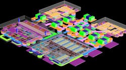
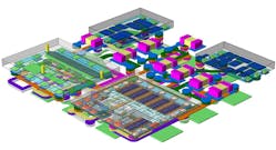
For RF modules that integrate multiple technologies developed with a range of tools, the need for greater interoperability between tools often goes beyond simple data-format compatibility due to the complexity of the overall design task. Front-end modules and other multi-technology devices can contain upwards of 25 integrated circuits (ICs) on a single laminate module, including BAW and SAW filters, III-V RF MMIC PAs, silicon switches with multiple antennas, and silicon LNAs. In this article’s design example, the silicon switches and LNAs were designed in Cadence and the acoustic/laminate filters were done in the Microwave Office software. Figure 1 shows what a typical multichip module design would look like.
1. Shown is a typical module design in the Microwave Office software.
A less-automated design flow would incorporate the performance of the RFICs modeled in Cadence Virtuoso using small-signal touchstone S-parameters, with one file for each switch state, or an MDIF with the switch state represented by a parameterized variable. Either approach requires large files that must be created, updated with any design changes, and then shared across design teams.
Creating the necessary files for all the needed switch states is time-consuming for the switch designer. The process could be error-prone in support of the more than 250 states covered by the RFIC. In the case of the touchstone files, only linear behavior is captured. The nonlinear behavior, which is critical to switches and even acoustic filters, would need to be captured by the larger polyharmonic file. With the RFIC analysis and S-parameter file generation taking seven minutes per state with 68 states for one switch and 25 states for the other, a huge time investment is required—one that would take hours or even days to generate.
Cadence Virtuoso and NI AWR Software Co-Simulation Flow
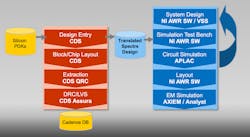
The solution featured in this article utilized new capabilities that support Cadence designs directly within the Microwave Office software. Figure 2 shows an overview of this flow. Here, a design flow based on the translation of the Cadence Spectre netlist within Microwave Office circuit simulation enables Cadence Virtuoso and NI AWR software co-simulation.
2. This diagram illustrates the Cadence Spectre translation flow for co-simulation in the NI AWR Design Environment platform.
The flow is made possible by taking the silicon process PDK in Cadence and translating both the PDK and design and transporting them via a Spectre design netlist into the Microwave Office software, where the designer has access to all NI AWR Design Environment tools. These tools include Visual System Simulator (VSS) system design software, Microwave Office linear and nonlinear simulation, APLAC harmonic balance and transient simulation, NI AWR layout tools, and AXIEM 3D planar and Analyst 3D finite-element method (FEM) EM simulators.
Figure 3 reveals the Cadence Virtuoso schematic for a double-pole/eight-throw (DP8T) silicon switch with on-die filter. The critical component is the antenna switch module (ASM), which has six different switch states.
3. This is a Cadence Virtuoso switch schematic.
Netlist and Run
Using the “Netlist and Run” command within Cadence will create the files needed for NI AWR software translation. Since this command is run from a test-bench level, the schematic that must be translated is actually a subcircuit. The most critical file created is input.scs, which contains all of the relevant Cadence schematic information.
Running the “Import Spectre Netlist Design” script will bring up a simple user interface dialog. Translation of this switch design (approximate 2,000-line netlist) took roughly one second. When the translation is complete, two components are available for use in any design: one for the process and the other for the actual design.
A log file is also generated that provides the designer and/or design support team with more detailed information concerning the cells that were translated, the libraries used, and the test-bench simulations. The translation includes microstrip-line (MLIN) elements from the original design, which provides accurate modeling of dispersion and loss in the transmission lines found within the design. In addition, directory paths to any files containing S-parameter blocks on the Cadence side are captured.
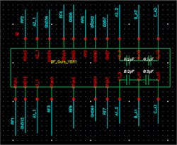
Once the switch design is translated, the user loads the two new PDKs into a new or existing project in Microwave Office software: the translated Cadence foundry PDK (csoi7rf global foundries PDK; Fig. 4, left) and the design PDK (RF-Core; Fig. 4, right). The RF Core file provides both the schematic element and the design block. These PDKs will provide three simple NI AWR software library elements needed for simulation.
4. The translated Cadence foundry PDK (left) and the design PDK (right) appear in the element tree library, ready for insertion in any NI AWR software design.
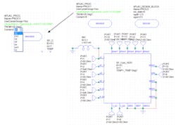
The new library elements are available through standard “drag and drop” placement into a Microwave Office circuit design software schematic, just like any other schematic element. Looking at the schematic view in Figure 5, the PROCESS block is used to reference the foundry PDK process and allows the user to alter the process corners. With the DESIGN block, the user can access any design variables within the Cadence design.
5. The PROCESS block (foundry PDK process) and the DESIGN block for the design variables from the Cadence design are visible in this Microwave Office schematic.
It can be seen on the right that this translated component has roughly 20 ports. The DESIGN block is where the switch state is controlled (set to 6 in this example), as well as the two voltages that will control the switch state. The PROCESS block on the top left (highlighted on the left side of the figure) provides designers with the ability to specify the process corners, which is very important for developing silicon IC designs.
To verify the frequency response of the netlist translation simulated in Microwave Office versus the original Spectre results, the S-parameters from a test-case Spectre simulation were imported into Microwave Office for comparison. The verification setup is virtually identical to the schematic test bench containing the translated netlist. For this simulation, the subcircuit contains the touchstone S-parameter block exported directly out of Cadence.
Comparing Small-Signal Results
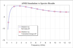
Figure 6 shows a comparison of the small-signal response (insertion loss) through a single path for the NI AWR software simulation of the translated netlist versus the Spectre results. This is represented by S-parameters across the entire frequency band. As expected, the results show exact agreement between the two results.
6. The small-signal results from the NI AWR software simulation are compared with the Spectre results.
Additional Analysis
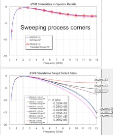
Now that the design translation has been verified, many other simulations can be performed with the switch, which includes sweeping the process corners, tuning/sweeping the switch state, and tuning/sweeping the control voltages. The imported RFIC behaves just like a regular Microwave Office element. On the left side of Figure 7, the swept process corners have been compared to reference data taken directly from Cadence, showing the impact of the process corners and the overlap between simulators.
7. Other simulations can now be run with the switch because it behaves like a regular Microwave Office element.
The right side of Fig. 7 reveals the simulated insertion loss for different switch states (through paths) in this example. The RFIC has been controlled through six different switch states. The different responses, depending on the switch state, are shown. The designer can now develop the laminate design details based on an accurate RFIC model easily changing states through parameter settings, which can be tuned or swept.
Furthermore, as the switch design is now a regular Microwave Office subcircuit, it can be combined with any other Microwave Office elements, EM structures, data files, and more. It’s possible to combine multiple technologies into a single Microwave Office project, enabling co-simulation across technologies, as well as layout integration. A single laminate module can contain and combine Si switches, III-V PA RFICs, acoustic filters, and more. The final integrated design layout includes acoustic filters along with Si-device, GaAs-PA, and module technology.
Assigning Layout
The switch layout can also be exported out of Cadence Virtuoso in a standard format like GDSII and imported into NI AWR software, where it can then be associated or linked with the schematic subcircuit to ensure proper layout connectivity (Fig. 8). The layout geometries are identical, with the colors being different simply as a matter of preference.
8. The switch layout is able to be exported out of Cadence Virtuoso and imported into NI AWR software, where it can then be associated or linked with the schematic subcircuit to ensure proper layout connectivity.
Conclusion
This article presented an integrated design flow for combining multiple technologies originating from different software tools into a single project, enabling co-simulation across simulation and layout design tools. This flow allows designers to not only integrate different semiconductor and packaging (laminate) technologies, but leverage complex designs that were originally created in a leading RFIC design environment for incorporation into a design environment specialized for MMIC, RF PCB, and module development. The final integrated design layout includes four different technologies: acoustic filters, a silicon device, a GaAs PA, and module technology.
