Download this article in PDF format.
5G is expected to offer extremely fast rates with extremely low latency. To achieve these tough specifications, the operating frequency must be in a region where high bandwidth and high speed is available. That means a move toward the millimeter-wave (mmWave) band.
The mmWave band had always been viewed as unsuitable for mobile communications, mainly due to high loss and propagation issues. However, research has shown that these propagation issues can be addressed and overcome with phased arrays and beamsteering antennas.
A phased-array antenna is composed of multiple radiating elements. Each element is connected to a phase shifter, which forms the beam that steers the antenna via constructive or destructive interference. Phased-array antennas allow engineers to enter the mmWave spectrum and achieve the high bandwidth and high speeds that 5G promises. Within the mmWave spectrum, the 28-GHz band has been chosen as one of the candidate bands to quantify 5G.
This article discusses the process involved in the design and simulation of a 5G 28-GHz phased-array transmit chain, as well as the theory behind each step in the process. Starting with electromagnetic (EM) circuit co-simulation, results and analysis that were uncovered during the design phase are detailed.
EM/Circuit Excitation and Co-Simulation
5G presents considerable design and simulation challenges, especially when combining high-frequency circuit design elements of multiple manufacturing technologies with different model abstractions including physical EM models. All of this must be combined and co-simulated simultaneously.
EM coupling from the physical designs and their interactions with other components in the system needs to be modeled and accurately accounted for. For this reason, 5G designers desperately need good tools that can integrate and co-simulate these models and technologies together and account for all their interactions, or else the simulation results will be off and result in product failure.
The EM/circuit excitation and co-simulation process in Keysight Technologies’ Advanced Design System (ADS) delivers such simulation and analysis criteria. It also plays an important role in delivering accurate simultaneous simulation and analysis of the whole transmit chain with all of its components, including the antenna.
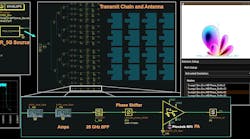
Figure 1 illustrates the EM/circuit excitation technique. The transceiver components on the schematic page are designed at the circuit level using foundry design kit models, or they’re represented by their S-parameter models, nonlinear X-parameter models, and EM models.
1. Shown is the EM/circuit excitation process in ADS.
The output of such circuit simulation on the transmit chain drives and excites the physical antenna structure that’s being simultaneously co-simulated with Momentum Planar EM solver or Full 3D FEM solver in ADS. The output response at the far right of Fig. 1 comprises the complete EM/circuit co-simulated results produced by capturing the excitation from the transmitter module and applying it directly to the antenna.
All simulated states of the phase shifter are exported to the output far-field results as shown at the far right of Fig. 1. The output beam and its side lobes and nulls can then be displayed and steered for any selected phase-shifter state. Thus, it contains the complete EM/circuit co-simulation and analysis results.
EM/Circuit Co-Simulation with Circuit Envelope
EM/circuit excitation and co-simulation work with all circuit simulators in ADS.1 However, using a circuit-envelope simulator in this process is essential because it allows for realistic 5G modulated sources to be applied at the input of the transmit chain and accurately outputs the results at the antenna.
5G signals by nature are time-varying complex modulated signals. Circuit envelope is a hybrid time- and frequency-domain simulator that can effectively handle and simulate these types of signals. When these signals drive the power amplifiers (PAs), the output at certain times consists of peak power values, while at other times consists of lower power values.
The peak-to-average ratio would compress the PAs in a complex fashion as compared to traditional steady-state harmonic balance with simplistic sinusoidal power sources. This helps designers uncover how much power must be backed off from the input of the PA to maintain the required linearity and meet the specifications. Circuit envelope is also much more efficient in memory when simulating modulated signals; it captures memory effects of the amplifiers and their effect on the spectrum power, error vector magnitude (EVM), and other measures.
In this EM/circuit co-simulation process with circuit envelope using 5G modulated sources, we are not abstracting models to co-simulate. Rather we are truly co-simulating the actual circuits with memory effects. The EM/circuit excitation truly captures the excitation from the TR module output and applies it to the antenna to get true and complete EM circuit simulation results.
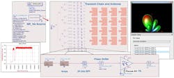
Figure 2 shows the simulation setup of the transmit chain using a 5G New Radio (NR) source with circuit-envelope simulation on the entire transmit chain. The output beam far-field plot is shown on the right for the phase shifter angle of 62° that corresponds to a 20° beam look-up angle.2
Transmit-Chain Components and Antenna
Figure 2 also illustrates the transmit-chain components of the 16 channels, all designed in ADS1 and connected to the patch antenna:
- The mmWave PA was designed by Plextek RFI (plextekrfi.com). It was implemented using Global Communication Semiconductors’ (GCS; www.gcsincorp.com) indium-phosphide (InP) dual heterojunction bipolar transistor (HBT) process. The PA provides 20 dB of gain at 28 GHz and achieves a 1-dB compression (P1dB) of +27 dBm. Its input and output voltage standing wave ratio (VSWR) is better than 1.2:1.
- The small signal amplifier was also designed by Plextek RFI. It was implemented using Qorvo’s (qorvo.com) pHEMT process. It provides 14 dB of gain with input and output VSWR better than 1.2:1.
- The power dividers and the mmWave four-bit phase shifters (with 22.5-deg. phase increments) were designed using Qorvo’s pHEMT process. The filter was implemented with lumped component models in ADS.
- The 28-GHz λ/2 patch antenna was designed on a Duroid substrate with VSWR better than 1.4:1.
2. This simulation features EM/circuit excitation on the entire transmit chain using a 5G New Radio source with circuit envelope.
More information concerning these component’s design and performance is provided in the referenced webcast.6
X-Parameter Models and 5G System Simulation
When designing and simulating 5G modules, X-parameters become extremely beneficial.3 Since its pioneering introduction in 2008, X-parameter technology has developed rapidly. While S-parameters provide a solution to small-signal linear devices, X-parameters solve nonlinear problems with higher input power. They can accurately capture all nonlinearities in nonlinear circuits such as the PA, including the fundamental, the harmonics, the intermodulation distortion, amplitudes, and phase. They accurately replicate the actual circuit design, resulting in much faster simulation time—especially during tradeoff analysis.
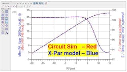
For example, Figure 3 clearly shows how the PA’s circuit-simulation results are identical to the X-parameter model simulation results in both amplitude and phase. Therefore, it’s advantageous to use X-parameter models during “what if” and “tradeoff” analysis. It runs much faster and provides protection to your IP if you prefer not to expose or share the topology of your circuit designs.
3. In this circuit simulation versus X-parameter model simulation, Pin/Pout and phase response of the PA is revealed.
5G Verification Test Benches in ADS
A verification test bench (VTB) is a regular component in the ADS simulation environment, which is linked to the VTB in SystemVue.4 VTBs enable circuit designers to make use of sources and measurement setups from SystemVue and verify the performance of a circuit using real-world complex modulated signals that conform to advanced wireless standards like 2G, 3G, 4G, and 5G.
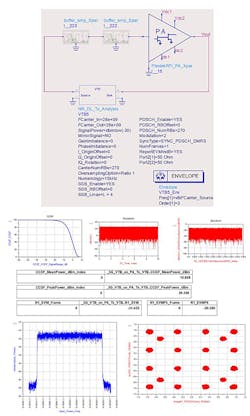
Placing a 5G VTB onto a schematic allows you to verify the transmit-chain components or the PA by itself with respect to 5G standards. The example in Figure 4 displays a VTB simulation setup for the two pre-amplifiers followed by the output PA in the transmit chain. The output display contains the complementary cumulative distribution function (CCDF) curve, the input and output spectrums, the mean and peak powers, EVM, constellation plot, and other measures.
4. VTB simulation setup and output results in ADS are given for the pre-amplifiers and PA in the transmit chain.
Experimentation and Analysis
Several experiments were performed using the EM/circuit excitation and co-simulation method to investigate the effect on the quality of the beam and its side lobes and nulls. Below is a summary of each analysis and its findings.
Effect of the Feed Network and Line Lengths
Feed network lines connect the PA integrated circuits (ICs) to the antenna ports. When all PAs are implemented on one IC, the outputs connect to the antenna patches with unequal line lengths and result in different and higher path losses and require calibration.
Described below is the effect of these unequal line lengths between the IC and the antenna patches prior to any calibration. This is something a design engineer would experience in the lab while prototyping and testing a system in its development stage.
To get a baseline reference, a simulation with no interconnect lines was initially performed. Figure 5 shows the result. The main lobe is perfectly centered at 0 deg. phase shift along the y-axis. The side lobes are 14.33 dB down and the nulls are 34.9 dB down.
5. This analysis uncovers the effect of the feed network and line lengths on the quality of the beam.
Next, feed lines of different lengths between the IC and the antenna patches were used to determine their effect on the beam. Using short lines (0.5 to 2 mm) resulted in shifting the beam by 5 deg., as shown in Fig. 5. The side lobes degraded and increased from −14.33 dB down to −8.9 dB down. The nulls degraded and went up from −34.9 dB down to −18.75 dB down.
A second experimental trial using longer lines (3 to 9 mm) was performed, resulting in drastic degradation in beam quality with a larger phase shift of 28 deg. The nulls and the lobes also went up. Fig. 5 tabulates the results.
This analysis clearly show that the lines can cause problems in the system. When working on a prototype, this issue comes up often. To avoid it, you must simulate and correct for it before building the system.
Effect of Varying the PA’s AM/PM Response
This experiment investigates the effect of having variation in amplitude and phase among all PAs used in the system. First, a simulation was performed with identical PAs to get a reference baseline of the beam quality with no variation. Next, several PAs with variation in their AM/PM response were utilized. The beam angle was not affected, but the influence on the lobes and nulls was prevalent.
The left side of Figure 6 displays the response of the PAs used in the experiment. Notice when the input RF power is +10 dBm, the corresponding Pout of the PAs varies by 3 dB and their phase varies by 3 deg. This variation in amplitude and phase has caused the distortion and degradation in the side lobes and nulls. Fig. 6 shows that the side lobes degraded and went up by 2 dB, while the nulls degraded and became at least 10 dB higher.
6. When various PAs with variation in AM/PM response are used in this experiment, side lobes are 2 dB higher and nulls are at least 10 dB higher.
Therefore, it’s very important to design the nonlinear components, such as the PAs, with small variation. Otherwise, unwanted results occur and cause problems in the overall system.
This leads to a discussion of a valuable statistical design technique that uses the “Design of Experiments” (DOE)5 to produce robust designs with minimum variation. To learn more about this technique, check out this video:
Figure 7 illustrates how the DOE methodology has transformed a PA with wide variation into one with smaller variation in both amplitude and phase.
7. The DOE methodology transformed a PA with wide variation into one with smaller variation in both amplitude and phase.
Effect of Coupling, Crosstalk, and Isolation
Coupling and crosstalk can occur between components in adjacent channels, either from adjacent PAs or from the antenna elements (usually accounted for by the EM simulation on the antenna). Coupling also appears on feed lines that connect the PAs to the antenna.
Similarly, crosstalk between two adjacent channels could occur, potentially leading to noticeable degradation in output signal quality. An RF signal in one channel would appear in an adjacent channel and cause interference and distortion.
An experiment on coupling effects was performed, first with no coupling between the channels in the transmit chain and then with coupling. The results showed similar degradation in the side lobes and nulls. The side lobes degraded and went up from −14.53 dB to −11.7 dB down from the main beam. The nulls degraded and went up from −36 dB to −19 dB down from the main beam.
Isolation is another key matter to consider. It’s crucial to design for good isolation between channels and avoid leakage from one channel to another as this could significantly affect the antenna element impedance. Designing for good isolation starts with making sure that all split-components in the system are designed well from the beginning. 5G systems contain several switches and splitters. It’s crucial to design these splitters, switches, and couplers with high isolation at the component level. It would eliminate many headaches at the end.
Effect of the PA Dynamic Impedance with the Antenna
As phase shifters control and change the beam-scan angle, the effective cross-section area of the array decreases because there’s less power to the main lobe and less directivity due to the wider beam. The PA loading and impedance changes, also referred to as “Active or Dynamic Impedance,” and can affect the final beam shape, and in extreme cases, may create blind spots as well.
In the April 15, 2011 technical note by Neill Tucker titled “An Introduction to Phased Array Design,” Tucker explains that the importance of active input impedance should not be underestimated. Its effects can be dramatic because they directly impact the amplitude and phase excitations of the array elements, and these are the very parameters you are using to control the array.
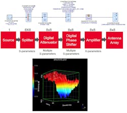
To explore this phenomenon, an 8-×-8 transmit chain was constructed and simulated in SystemVue (Fig. 8).4 Mild blind spots can be seen at certain azimuth and elevation scanned angles. The main beam is seen to drop down by 3 dB at these specific angles. Under different conditions, different active impedance between the PAs and the antenna could result in full blind spots of the beam. Designers, therefore, should not underestimate it and must give it considerable attention.
8. This SystemVue test case on dynamic impedance shows blind spots at certain azimuth and elevation scanned angles.
Conclusion
The design, simulation, and analysis of a 5G 28-GHz phased-array transmit chain was demonstrated. The EM circuit excitation and co-simulation process in ADS using realistic 5G NR input sources and X-parameter models was thoroughly described. It was shown to be practical, powerful, and efficient, especially during the system design, analysis, and development phase. Various design-related analyses were performed with interesting and useful results to the design engineers. For more information, readers are encouraged to check out the live webcast recording that was given on this topic.6
Acknowledgement
The author would like to acknowledge Plextek RFI design center for providing both small-signal and PA designs that were used in the transmit-chain design and analysis. He would also like to acknowledge Anil Panday and Rupam Anand of Keysight Technologies for their help and support in this project.
Jack Sifri is the MMIC/Module Design-Flow Specialist and Product Manager of MMIC simulation technologies at Keysight EEsof EDA.
References
- Keysight Technologies Advanced Design System (ADS).
- eu; Phased Array Antenna and Radar Basics.
- Keysight Technologies X-Parameters: https://www.keysight.com/main/application.jspx?cc=US&lc=eng&nid=-34017.0 https://www.keysight.com/main/editorial.jspx?cc=US&lc=eng&ckey=1780767&nid=-33395.0&id=1780767
- Keysight Technologies SystemVue.
- Keysight Technologies YouTube video on “How to Use Design of Experiments to Create Robust Designs with High Yield.”
- Keysight Technologies “Design and Simulation of 5G 28-GHz Phased Array Transceiver.” August 3, 2017 Webcast.
