My recent blogs have focused on MIMO phased-array designs. I want to take a slight diversion and share another interesting workflow, but on a much smaller scale. You can now fabricate printed-circuit-board (PCB) antennas with MATLAB and Antenna Toolbox. This can be done for arbitrary metal-dielectric layers, solid feed/via models, and different connector types.
There are several ways to get started. You can define the geometric shape of your metal structures. You can start with an antenna element from the built-in library in Antenna Toolbox. Or you can even import your design starting with a photo of an existing antenna, which I will write about in a future blog.
For this blog, the design is for an L-band system with a bandwidth of about 17% of the carrier frequency. Using this design, I will generate a set of Gerber files for a PCB antenna from MATLAB. To show this workflow, we start with a model of a microstrip-fed printed wide slot antenna on an FR4 substrate.
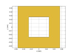
This antenna has two metal layers on either side of a single-layer PCB. The first metal layer is the microstrip feedline, and the second layer of metal is the ground plane with a wide slot cut out from it. The ground plane geometry is shown in Figure 1.
1. Shown here is the antenna’s ground plane geometry.
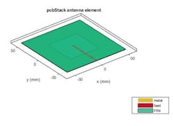
The PCB stack is defined using the dielectric material and arranging the layers in a top-down description, starting with the top-most layer of metal. Both the feed location and diameter are defined as well. This antenna has the microstrip feedline brought out to the edge of the board as shown in Figure 2.
2. This is the microstrip antenna with feedline.
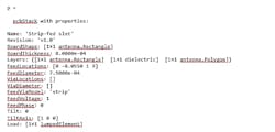
The properties of the PCB stack are as follows:
In the next step, you generate the Gerber files for the PCB’s geometry information. To generate these files, two additional pieces of information are required apart from the PCB itself. The first is the connector type; the second is the PCB manufacturing service/viewer service. The type of RF connector determines the pad layouts on the PCB. You can select these from a catalog of PCB services and RF connectors provided in Antenna Toolbox. The PCB services catalog supports configuring the Gerber file generation process for manufacturing as well as for online viewer-only. The code for this example is as follows:
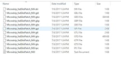
The files are generated as illustrated in Figure 3.
3. The design files are generated for the antenna PCB.
Figure 4 shows this design rendered within the Mayhewlabs free 3D online Gerber viewer.
4. Shown is the PCB design for the front and back, rendered in Gerber viewer.
You can then configure the Gerber file generation process for the Seeed Fusion PCB manufacturing services:
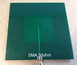
Figure 5 shows the antenna we received from this design.
5. Here’s a photo of the prototype antenna.
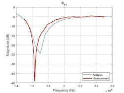
The S11 reflection coefficient of the prototype antenna was measured in the Antenna Lab at Worcester Polytechnic Institute (WPI). The results comparing the design analysis and the measured performance are plotted in Figure 6.
6. Design analysis and measured S11 results are plotted.
The agreement between the analyzed and measured results is reasonable, with approximately 4% absolute error in the S11 minimum.
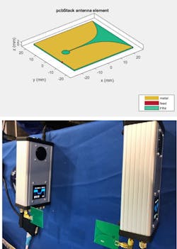
I want to share another example we implemented using this workflow. At the International Microwave Symposium (IMS) 2018 in Philadelphia, we built a directional antenna to use as part of a demo we did with Analog Devices. Figure 7 shows the PCB design in Antenna Toolbox along with two portable radio prototypes we used to send data packets between devices. A Vivaldi antenna was utilized because of the increase in directivity over the omnidirectional monopole antenna that comes with the radio. Just a few weeks before the conference, my colleague designed the antenna and had it printed in time for the conference. It worked great and helped us with our demonstration.
7. The PCB antenna for a Vivaldi antenna is shown, along with two portable radio prototypes.
Learn more about the topics covered in this blog:
PCB Antenna Design, Simulation, and Fabrication with MATLAB (Video): Learn how to design PCB antennas with Antenna Toolbox and generate Gerber files used to describe PCB antennas.
Design, Analysis and Prototyping of a Microstrip-Fed Wide Slot Antenna (Example): Learn to build a model of a microstrip-fed printed wide slot antenna on FR4, analyze it, and prototype the antenna by generating Gerber files.
Antenna Array Analysis with Custom Radiation Pattern (Example): Learn to import a custom antenna radiation pattern and then analyze the array's response pattern. The pattern can be either from a measurement or from simulation.
See additional 5G, radar, and EW resources, including those referenced in previous blog posts.
