


Advanced defense electronics systems often start with microscopic devices like semiconductors as building blocks, and that’s certainly the case with Northrop Grumman and its high-volume, high-frequency semiconductor foundry. In addition to selling semiconductor devices such as amplifiers and transistors fabricated in the foundry, the company offers foundry services for its gallium-arsenide (GaAs), gallium-nitride (GaN), and indium-phosphide (InP) wafer processes. Thus, customers can try their own monolithic-microwave-integrated-circuit (MMIC) designs on these state-of-the-art, high-volume microwave/millimeter-wave semiconductor processes.
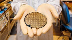
The high-volume semiconductor foundry (Fig. 1) constructs MMICs using heterojunction bipolar transistors (HBTs) and pseudomorphic high-electron-mobility transistors (pHEMTs), depending on the process. Each process starts with a 100-mm-diameter wafer, enabling customers to achieve a healthy volume of MMIC devices for a successful run. To improve the chances for a successful run, final design rule checks (DRCs) are performed by foundry personnel, who have more than a little experience on the requirements for each process.

1. The Redondo Beach, Calif. semiconductor foundry houses several different device processes for fabricating microcircuits with low noise figure, wide bandwidth, or high power at microwave and millimeter-wave frequencies.
The various foundry processes share a number of features, including availability of air-bridged metal and back-side viaholes for all processes, and the ability to implement Schottky diodes in all processes. As a DoD Trusted Foundry, the facility relies on mature computer-aided-engineering (CAE) models within leading software simulation tools, such as Keysight Technologies’ Advanced Design System (ADS) and the Microwave Office from National Instrument (NI)/Applied Wave Research (AWR), as well as extensive on-wafer measurement capabilities well into the millimeter-wave frequency range.