Download this article as a .PDF
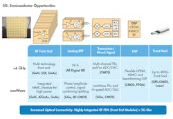
The advent of 5G has spurred a rethinking of wireless infrastructure, from semiconductors (Fig. 1) to base-station system architectures to network topologies.
At the semiconductor level, the mainstream commercialization of gallium-nitride-on-silicon (GaN-on-Si) has opened the door to improved RF power density, space savings, and energy efficiency. These improvements come at affordable cost structures that are on par with LDMOS at scaled volume production levels, as well as far below GaN-on-silicon-carbide (GaN-on-SiC).
In parallel, the use case for GaN has expanded beyond discrete transistors for high-power RF applications. The economies of scale achieved with GaN’s propagation into commercial 4G LTE wireless infrastructure has enabled GaN’s migration into the monolithic-microwave-integrated circuit (MMIC) market, where it’s helping system designers achieve higher levels of functionality and device integration for next-generation 5G systems.
1. This figure illustrates the different semiconductor technologies that figure to play a role in 5G.
Meanwhile, the evolution of RF systems-on-a-chip (SoCs) with integrated RF, analog, and digital circuitry has unlocked huge gains in data processing speed across a very wide frequency range, leveraging advanced direct sampling capabilities. At the board level, this eliminates the need for discrete data converters tied to very specific frequency plans, enabling smaller system footprints with digital flexibility and increased input/output (I/O).
At the network node level, 5G data throughput requirements invite a fresh look at the optical transport technologies tasked with offloading and routing the 5G data deluge. By taking a holistic view of the network from base stations to network fiber optics—from RF to light, if you will—system designers can gain a better understanding of the challenges and opportunities that arise when these technologies intersect.
Here, we will assess the benefits of GaN-on-Si for integrated, multi-function MMICs, as well as the benefits of RF SOCs and advanced optical technology architectures that are affecting the evolution of 5G wireless infrastructure.
Innovation in GaN and MMICs
The sheer density of massive multiple-input, multiple-output (MIMO) antenna configurations—scaling in excess of 256 transmit and receive elements in a single 5G base station—puts a premium value on available printed-circuit-board (PCB) space, particularly at higher frequencies. To meet this challenge, multi-function MMICs are supplanting discrete integrated circuits (ICs) and single-function MMICs in 5G base-station designs.
In addition to the benefits in space savings that multi-function integration helps to drive, costs are lowered through a reduction in individual die packaging, design complexity, testing, and assembly labor. Reducing the number of interfaces improves overall mechanical reliability.
Against this backdrop, GaN-on-Si’s successful penetration into the commercial semiconductor marketplace comes at a fortuitous time (Fig. 2). Its scalability to 8- and 12-in. silicon wafers is enabling cost efficiencies that are well out of reach for GaN-on-SiC, at power densities that can’t be achieved with LDMOS—upward of 4× to 6× more power per unit area.
2. GaN-on-Si technology is already significant in terms of today’s commercial market.
Bridging the gap between these two key attributes, GaN-on-Si is further distinguished by its ability to integrate increased functionality at the silicon level, yielding additional space optimization for ultra-compact MMICs. Its silicon substrate supports homogenous integration of GaN devices and CMOS-based devices on a single chip—a capability that GaN-on-SiC cannot provide due to the inherent process limitations. This opens the door to multi-function, digitally-assisted RF MMICs that can incorporate on-chip digital control and calibration, on-chip power distribution networks, and more.
RF SoC Processing Efficiency
For 5G base-station infrastructure, the integration benefits and reductions in hardware content enabled by GaN-on-Si-based multi-function MMICs are further complemented by the recent commercial-market emergence of RF SoCs. Integrating multi-Gsample RF data converters for high-speed data processing across a very wide frequency range, RF SoCs streamline the data pipeline and provide a scalable pathway for increasing RF channel-count.
With conventional superheterodyne receiver architectures, signals have to be downconverted to baseband signals, which requires a mixer and additional circuitry. A 2.6-GHz RF signal (4G LTE) would need to be downconverted to the MHz frequency range, where a conventional analog-to-digital converter (ADC) could sample at a lower speed.
In order to place all of the frequency content in the first Nyquist band, you need to sample at 3× the radio frequency. A 2.6-GHz signal would need to be sampled at almost 8 Gsamples/s to achieve this, far outstripping the capability of conventional ADCs sampling at much lower rates—typically 3 Gsamples/s in the 400-MHz frequency range.
A new generation of RF SoCs is overcoming this obstacle, providing the ability to sample signals at up to 56 Gsamples/s. This capability enables direct RF sampling at very high RF frequencies, with the option to down sample. This digital sampling capability eliminates the need for a conventional superheterodyne receiver and discrete data converters, while also eliminating the exciter technology needed for superheterodyne sampling.
RF SoCs can pack a very large number of channels into a very small footprint. Functionally, anywhere from 4 to 16 channels can be fitted into an IC that is approximately 12-×-12 mm instead of requiring multiple circuit cards to do the same thing. This is analogous to the footprint reductions and I/O gains achieved via the evolution from rotary phones to mobile smartphones. And with a defined pathway toward RF CMOS technology at 7-nm spacing, channel density will only continue to grow and power optimization will continue to improve.
Going forward, RF SoCs will enable signals that are increasingly free of distortion—ambiguities and imperfections that previously weren’t correctable will be readily correctable. At the system level, here again we see how the benefits of multi-function integration and reduced component count can drive significant space, power, and cost savings for affordable 5G infrastructure.
Also noteworthy, RF SoCs play a key role in the enablement of coherent beamforming, an active phased-array antenna technique used in advanced radar systems that can improve the performance of sub-6-GHz wireless base stations. With coherent beamforming, each transmit and receive element in a massive MIMO array operates in concert with others to dynamically increase transmitted power and receiver sensitivity in the direction of subscribers. This mitigates noise, interference, and reflections from other sources. Leveraging a combination of GaN-on-Si, heterolithic microwave integrated circuits (HMICs), and coherent beamforming technologies, system designers can enable high levels of energy efficiency within the tight size constraints of massive MIMO arrays.
From RF to Light
Wireless network operators and hyperscale data center operators share a common imperative on the pathway to 5G: They need to move data as quickly and cost efficiently as possible. As parallel advancements in RF and optical technologies begin to intersect and integrate, we will gain a clearer perspective of how innovations in one technology domain can affect the evolution of the other.
The faster data processing and throughput speeds achieved at the RF base station are likewise mirrored in the transition from 100G to 400G optical transceiver modules. This is particularly the case in the data center where port density must continue to increase to keep pace with insatiable data demands.
The broader trend toward higher levels of integration and reduced component count is a key factor in the evolution to 400G modules, where the emergence of the single lambda (aka single wavelength) PAM-4 modulation scheme is transforming module architectures. For 100G transceivers, single lambda PAM-4 technology can reduce the number of lasers to one, and eliminates the need for optical multiplexing.
For 400G implementations, only four optical assemblies are needed, representing a major opportunity for data center operators to reduce their cost with an extremely compact and energy-efficient module. This innovation in the hyperscale data center will emanate outward to wireless network nodes in the not-too-distant future.
3 . This figure points out some noteworthy factors associated with 5G.
At the semiconductor level, accelerating advancements in silicon photonics technology will transform the composition of next-generation, multi-function MMICs, leveraging established CMOS processes to generate thousands of optical components at a time when on-wafer substrates are leveraging commercial-scale manufacturing techniques. With newfound ability to integrate GaN-based RF devices together with optical devices on a single silicon die—at extremely attractive cost structures—the resulting reduction in interfaces between RF and optical componentry will make it that much easier to push cleaner, faster signals through the network.
In the meantime, continued advancements in GaN-on-Si technology, multi-function MMICs, and RF SoCs will propel the RF/microwave industry toward the realization of more elegant, integrated, and cost effective wireless system infrastructure on the path to 5G connectivity (Fig. 3).


