This file type includes high resolution graphics and schematics when applicable.
Microwave power dividers/combiners are growing in importance, as evidenced by their increased use in antenna feeder networks, in power amplifiers, and with mixers in wireless communications systems. For effective and efficient use of available spectrum, dual-band and tri-band power divider circuits are being developed for these systems to combine the functions of two or three components, respectively, within one unit.
With the proliferation of dual-band requirements in wireless communication systems, several dual-band Wilkinson power dividers have been developed.1 One design employs asymmetric transmission lines,1,2 but within a complex structure. The most common multiple-band power-divider design is formed using two-section transmission lines with two lumped resistors at the end of the lines.3
Some designs using lumped inductors (Ls), resistors (Rs), and capacitors (Cs) at the output port to improve the port isolation have been proposed.4,5 However, the lumped reactive components—the inductor and capacitor—usually increase the parasitic effects between the output ports at higher operating frequencies.3 Designs based on microstrip coupled lines were proposed, but each of these designs suffered some shortcomings.6,7 To overcome the shortcomings of these previous dual-band power dividers, a new type of dual-band Wilkinson power divider with open stub at the output port was developed to aid the many expanding wireless communications applications.
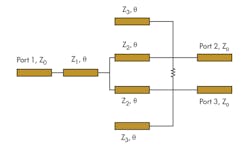
Figure 1 shows the topology of the proposed Wilkinson power divider. The characteristic impedances of the three transmission lines are denoted as Z1, Z2, and Z3; the lengths of the transmission lines are represented by L1, L2, and L3, respectively. Transmission line Z3 is used for phase compensation. The power divider can achieve good impedance matching and good isolation in two separate frequency bands—an ideal solution for many multiple-band wireless applications.
Obtaining the circuit parameters for the power divider was a matter of using odd-even-mode analysis and applying microwave network theory. Following that, commercial microwave simulation software would be used to simulate the behavior and performance of the circuit, and a physical example of the circuit design would be made for measurement purposes.
Because the power-divider circuit is symmetrical with respect to the middle line between the two output ports, there is no current flowing through the lumped components between the output ports in the even-mode situation. As a result, it is possible to produce the equivalent circuit shown in Fig. 2 for the microwave power divider. To facilitate the analysis, all impedance values were normalized to 50 Ω of the port impedance.
By applying microwave network theory, the equality for the ABCD matrix is given by Eq. 1:
According to the relationship between the change in impedance and the ABCD matrix, in order to impedance match ports 1 and 2 of the power divider design, Eq. 2 must be satisfied for the input impedance, Zin:
Zin = (AZ + B)/(CZ + D) = 2Z (2)
By solving Eqs. 1 and 2, Eqs. 3 and 4 can be obtained:
(Z22Z3 - 2Z21Z3 - 2Z21Z2 - Z1Z22)tan2θ - Z1Z2Z3 = 0 (3)
Z2Z3 + 2Z1Z3 +2Z1Z2 - Z22an2θ - 2Z21Z2Z3 - Z1Z22Z3 = 0 (4)
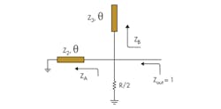
Figure 3 offers an equivalent circuit for the odd-mode analysis. In the odd-mode situation, there is a virtual ground in the middle of the two output ports, and impedance Z1 doesn’t work in this mode. Without the open stub, it is impossible to achieve impedance matching with this configuration.
From Fig. 3, the impedances of ZA and ZB can be written as:
ZA = jtanθ (5)
ZB = -j(Z3/tanθ (6)
To achieve impedance matching, impedances ZA and ZB must satisfy Eq. 7:
1/ZA + 1/ZB + 2/R = 1 (7)
By substituting Eqs. 5 and 6 into Eq. 7 and equating the real and imaginary parts, Eq. 7 can be reduced to Eqs. 8 and 9:
R = 2 (8)
tan2θ = Z3/Z2 (9)
Dual-band analysis was performed on the power-divider design in the following way. Assuming that the center frequencies of the proposed power divider can be found at frequencies f1 and f2, and f2 is greater than f1, they can be made equivalent by means of the factor k, where f2 = kf1 (k > 1). For the purpose of working in two center frequencies and bands, Eqs. 3, 4, 8, and 9 should be constructed around both center frequencies f1 and f2. Eq. 10 should then be satisfied, where:
tan2θf1 = tan2θf2 (10)
From Eq.10, Eqs. 11 and 12 can be obtained for θ:
θf1 = π/(1 + k) (11)
θf2 = kπ/(1 + k) (12)
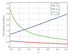
According to that given operating frequency ratio, k, by solving nonlinear equations Eqs. 3, 4, and 9, the values of impedances Z1, Z2, and Z3 can be obtained. Figure 4 shows the relationship between impedances Z1, Z2, and Z3 and the frequency ratio k. From Fig. 4, it can be seen that the dual-band power divider can be realized within a relatively wide frequency range.
To verify the design method presented for this Wilkinson power divider, an actual power divider was designed and fabricated. Target parameters were set by choosing f1 = 1 GHz and f2 = 3 GHz, then k = 3. The electrical lengths of the lines were θ1 = π/4 at f1 and θ2 = 3θ/4 at f2. By substituting tanθ = 1 into Eqs. 3, 4, and 9, it can be found that Z1 ≈ 0.486 × 50 = 24.295 Ω, Z2 ≈ 1.5742 × 50 = 78.62 Ω, Z3 = Z2, and R = 2 × 50 = 100 Ω. Using a microstrip line calculator, the length and width for each microstrip line needed to achieve these impedances was calculated.
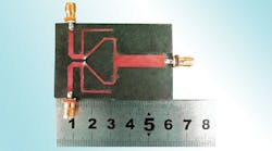
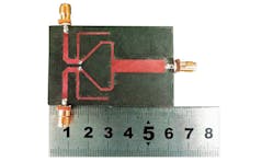
The power divider that was fabricated as a result is shown in Fig. 5. In the experiments, RT/5880 circuit-board material from Rogers Corp. was used as the substrate material. This circuit material includes a relative dielectric constant (εr) of 2.2 in the z-direction (thickness) with a tanδ of 0.0009. The thickness of the substrate dielectric layer was 0.787 mm and the conductor thickness was 0.018 mm.
This file type includes high resolution graphics and schematics when applicable.
Conclusion
This file type includes high resolution graphics and schematics when applicable.
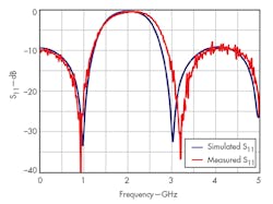
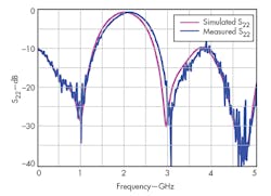
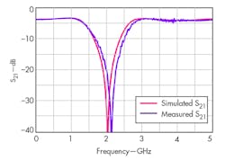
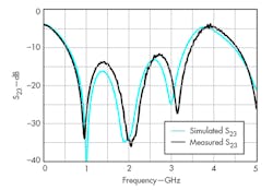
Scattering parameter measurements were performed using a model N5244A vector network analyzer (VNA) from Agilent Technologies (now Keysight Technologies) over the frequency range from 0.02 to 5 GHz. Figures 6 through 9 show the frequency responses of the divider in which the center frequency of the lower and upper bands were found not to be equal in the simulated and measured situation, respectively. The discrepancies between the simulated and measured results were mainly caused by the limited accuracy of the simulation processes used.
Moreover, Figs. 6 and 7 show that the input and output return loss were better than 22 dB at the power divider’s two center frequencies. Figure 8 shows that the insertion loss was less than 0.4 dB across the full frequency range of testing, while Fig. 9 reveals that the port isolation exceeded 27 dB.
In short, this dual-band power divider incorporates stub lines at the ends of the transmission lines for consistent performance over broad frequency ranges. The range of lower and upper band frequency ratios as presented for this power divider design could extend from 2 to 6. An even greater ratio is possible by changing the width of the impedances Z1, Z2, and Z3. The power divider can deliver good performance at any two frequencies.
The design only uses one lumped element and the resistance is 100 Ω at any frequency. Without the use of lumped reactive components, the effects of parasitic circuit elements were minimal, allowing the design to operate at higher frequencies if desired or required. The output port isolation was only related to the length and width of the transmission line Z2 and the stub line Z3 relatively.
Acknowledgment
This work was supported by the National Natural Science Foundation of China under grant No. 61001012.
Qing-Hua Tang, Professor
Bin-Qiao You, Master’s Degree Candidate
Zhi-Qing Xie, Engineer
Laming Zhan, Professor
Institute of Microwave Technology Application, Huazhong University of Science and Technology, Wuhan, 430074, People’s Republic of China
References
1.Yongle Wu, Yuanan Liu, Yaxing Zhang, JinchunGao, and Hui Zhou, “A Dual Band Unequal Wilkinson Power Divider Without Reactive Components,” IEEE Transactions on Microwave Theory & Techniques, Vol. 57, No. 1, December 2008, pp. 216-222.
2. M.-J. Park, “Dual-band unequal power divider with simplified structure,” IET Microwaves, Antennas & Propagation, Vol. 5, No. 15, December 2011, pp. 1891-1896.
3. Suyang Shi and Wenquan Che, “Dual-band power divider based on double-side parallel strip line (DSPSL),” China-Japan Joint Microwave Conference Proceedings (CJMW), 2011, pp.1-4.
4. Xiaolong Wang, I. Sakagami, K. Takahashi, and S. Okamura,” A Generalized Dual-Band Wilkinson Power Divider With Parallel L, C, and R Components,” IEEE Transactions on Microwave Theory & Techniques, Vol. 60, No. 4, February 2012, pp. 952-964.
5. L. Wu, H. Yilmaz, T. Bitzer, A. Pascht, and. M. Berroth, “A Dual-Frequency Wilkinson Power Divider: For a Frequency and Its First Harmonic,” IEEE Microwave & Wireless Components Letters, Vol. 15, No. 2, February 2005, pp. 107-109.
6. Y.-C. Liu, W.-H. Chen, X. Li, and Z.-H. Feng,” Compact design of dual-band power divider with coupled-line shunt elements,” Electronics Letters, Vol. 47, No. 4, February 2011, pp. 262-263.
7. Yucheng Liu, Wenhua Chen, Xiang Li, and Zhenghe Feng, “Design of Compact Dual-Band Power Divider With Frequency-Dependent Division Ratios Based on Multisection Coupled Line,” Components, Packaging, and Manufacturing Technology, Vol. 3, No. 3, January 2013, pp. 467-475.
This file type includes high resolution graphics and schematics when applicable.
