This file type includes high resolution graphics and schematics when applicable.
A power divider with bandpass response and high isolation between ports was developed for use in ultrawideband (UWB) communications systems. The design, which incorporates two slotline resonators, achieves excellent amplitude and phase balance between channels and ports.
Featuring a frequency range of 3.8 to 10.0 GHz, is well suited for UWB applications. One of the resonators helps improve isolation between output ports, while the other helps generate a tunable transmission zero so that a wide upper stopband could be obtained.
Interest in UWB systems and components has increased steadily since about 2002, when UWB communications systems concepts were first introduced and developed. A number of components for UWB applications have been designed and fabricated since that time.1-6 Power dividers are among the most crucial of RF/microwave devices, since signals must be split and channeled through communications signals for proper detection and processing.
To meet the requirements for UWB systems, a number of UWB power dividers have been developed, with different configurations based on traditional Wilkinson power dividers.7-9 For the sake of shrinking the dimensions of power dividers for UWB applications, slotline techniques have been studied and applied. As an example, a single-wavelength slotline was applied to structure a noncoplanar, in-phase UWB compact power divider with a flat passband over the UWB frequency range.10 By adding one circular stub at the end of each output branch as compensatory circuits, it was possible to extend the operating frequency range of the power divider, and also helped to achieve a flat passband.11,12
However, due to the inherent properties of three-port networks, a lossless and reciprocal three-port network cannot obtain good impedance matching at all ports simultaneously. As a result, for the UWB power divider designs that had been developed with slotline techniques, the impedance matching at the output ports was poor, with low isolation between output ports.
Even worse, the bandwidths of the stopbands for these designs were relatively narrow,13,14 enabling undesired signals to enter into systems employing these UWB power dividers. Of course, additional filtering can be added to the systems to suppress the unwanted signals, but this adds to the cost of the system.
To meet the needs of UWB systems for power dividers at reduced costs and compact sizes, a novel compact in-phase multilayer power divider with wide stopband was designed using slotline techniques. The output branches of the proposed UWB power divider are placed on the same layer symmetric to the input arm to achieve in-phase output signals.
To improve the impedance-matching limitations that are traditionally suffered by UWB power dividers based on slotline techniques, an isolation resistor was added to the power divider circuitry as used in a traditional Wilkinson power divider. To obtain a wide stopband with the power divider, a one-half-wavelength slotline resonator was placed at the input port to generate another transmission zero in the stopband, resulting in a wide stopband range.
The results from computer simulations and measurements agree quite closely for this UWB power divider, showing that the multilayer circuit design achieves good impedance matching at all ports, with high isolation between ports and excellent amplitude and phase balance between output ports over the UWB frequency range from 3.8 to 10.0 GHz.
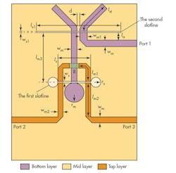
Figure 1 shows the configuration of the proposed in-phase UWB power divider, which consists of three layers (top, middle, and bottom layers). The input port (1) is located in the bottom layer, while the output ports (2 and 3) are placed in the top layer. The slotlines are etched in the middle layer, which is the ground plane. The length of the first slotline is decreased relative to slotlines used in previous UWB power-divider designs so that an isolation resistor could be installed at the ends of the output branches.
Two short-circuited circular slotline stubs and one open-circuited circular microstrip stub, which act as compensatory circuits, were included to reduce passband amplitude ripple. The short microstrip stubs at the ends of the output branches can also help increase the passband flatness, at the same time making installation of the isolation resistor easier.
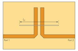
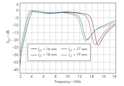
Figure 2 shows the half-wavelength slotline resonator, consisting of a UWB filter with microstrip lines. This filter can achieve several transmission poles for an UWB operating frequency range and generate one transmission zero at stopband. By adjusting the length of the slotline, the transmission zero will shift towards a high-frequency band or a low-frequency band. Figure 3 offers simulated results for the UWB filter designed for this power divider, indicating that the transmission zero will move toward the lower-frequency band with increasing length and move toward a higher-frequency band with decreasing length.
The prototype multilayer in-phase power divider with bandpass response and high isolation was designed and fabricated on 4350B printed-circuit-board (PCB) material from Rogers Corp. with relative dielectric constant of 3.48, loss tangent of 0.0037, and thickness of 0.508 mm. Figure 4 shows photographs of the proposed power divider. The size of the fabricated power divider is 24 × 30 mm.
This file type includes high resolution graphics and schematics when applicable.
Simulating the Divider
This file type includes high resolution graphics and schematics when applicable.
The UWB power divider was computer simulated with the aid of Version 13.0 High Frequency Structure Simulator (HFSS) electromagnetic (EM) finite-element simulation software from ANSYS Corp. The dimensions of the power divider’s parameters from the simulation software (and as detailed in Fig. 1) are: wm = 1.15 mm, wm1 = 1.4 mm, wm2 = 0.91 mm, d = 0.5 mm, lst = 6.92 mm, la = 1.72 mm, ls1 = 16.09 mm, ls = 6.21 mm, lm1 = 4.93 mm, lm2 = 6.64 mm, lm3 = 9.62 mm, ws = 0.23 mm, ws1 = 0.26 mm, rs = 0.93 mm, and rm = 1.86 mm. The isolation resistor is R = 100 Ω. For the sake of compatibility with other systems, the port impedances are fixed at 50 Ω.
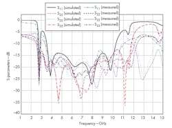
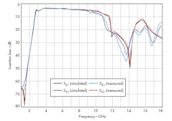
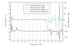
Figures 5, 6, and 7 provide comparisons of simulated and measured results for the UWB power divider, showing fairly good agreement across the wide frequency range. In fact, light differences can be traced from machining errors. The measured return losses are more than 17 dB for port 1, more than 15.5 dB for port 2, and more than 15.4 dB for port 3 across the frequency band from 3.8 to 10.0 GHz. Isolation between output ports is better than 16 dB. Insertion losses, including losses from SMA connectors, are about 1 ± 0.7 dB and 1 ± 0.6 dB. The amplitude unbalance is ±0.2 dB for the same frequency range while the phase unbalance is about ±2 deg.
In addition, the group delay exhibits good flatness across the bandwidth, with maximum difference of just 0.13 ns across the wide frequency band. Signal suppression is about 20 dB for the frequency band from 11.5 to 17.5 GHz, and attenuation reaches 20 dB at 2.5 GHz, ensuring that the power divider can reject undesired signals.
As was demonstrated, it is possible to construct a novel in-phase multilayer power divider with a bandpass response and high isolation by using slotline techniques. The width of the stopband was successfully extended by introducing a one-half-wavelength slotline resonator to the power-divider circuitry. The measured and simulated results for the UWB power divider show good impedance matching at all ports by introducing one resistor at the ends of the output branches. The UWB power divider shows good amplitude and phase balance between its output ports from 3.8 to 10.0 GHz, making it a suitable candidate for a variety of UWB applications.
Acknowledgments
This work was sponsored by the National Natural Science Foundation of China (Grant No. 61006026) and the Fundamental Research Funds for the Central Universities (Grant No. ZYGX2012J030).
Long Xiao, Engineer
School of Electronic Engineering, University of Electronic Science and Technology of China, Chengdu, People’s Republic of China, 611731
Hao Peng, Engineer
School of Electronic Engineering, University of Electronic Science and Technology of China, Chengdu, People’s Republic of China, 611731
Tao Yang, Engineer
School of Electronic Engineering, University of Electronic Science and Technology of China, Chengdu, People’s Republic of China, 611731
References
1. A.M. Abbosh, “Ultra-wideband three-way power divider using broadside-coupled microstrip-coplanar waveguide,” Microwave and Optical Technology Letters, Vol. 54, No. 1, January 2012, pp. 196-199.
2. M.A. Sanchez-Soriano and G. Torregrosa-Penalva, “Compact UWB bandpass filter based on signal interference techniques,” IEEE Microwave and Wireless Components Letters, Vol. 19, No. 11, November 2009, pp. 692-694.
3. C.L. Hsu, F.C. Hsu, and J.T. Kuo, “Microstrip bandpass filters for ultrawideband (UWB) wireless communications,” IEEE MTT-S International Microwave Symposium Digest, June 2005, pp. 12-17.
4. H. Shaman and J.S Hong, “Ultrawideband (UWB) bandpass filter with embedded band notch structures,” IEEE Microwave and Wireless Components Letters, Vol. 17, No. 3, March 2007, pp. 193-195.
5. A.K. Gautam, S. Yadav, and B.K. Kanaujia, “A CPW-fed compact inverted L-strip UWB microstrip antenna,” IEEE Antennas and Wireless Propagation Letters, Vol. 12, 2013, pp. 151-154.
6. P.N. Shinde and B.K. Mishra, “Compact thin ground plane UWB antenna with dual band stop characteristics,” Microwave and Optical Technology Letters, Vol. 55, No. 5, May 2013, pp. 1045-1049.
7. C.L. Zhuge, K.J. Song, and Y. Fan, “Ultra-wideband (UWB) power divider based on signal interference techniques,” Microwave and Optical Technology Letters, Vol. 54, No. 4, April 2012, pp. 1028-1030.
8. A.R. Hazeri, “An ultrawideband Wilkinson power divider,” International Journal of Electronics, Vol. 99, No. 4, April 2012, pp. 575-584.
9. L. Chen, F. Wei, C.J. Gao, and W.Q. Wu, “UWB power divider with one narrow notch-band and wide stop-band,” Microwave and Optical Technology Letters, Vol. 55, No. 3, March 2013, pp. 597-600.
10. K.J. Song and Q. Xue, “Ultra-wideband out-of-phase power divider using multilayer microstrip-slotline coupling structure,” Microwave and Optical Technology Letters, Vol. 52, No. 7, July 2010, pp. 1591-1594.
11. M.E. Bialkowski and A.M. Abbosh, “Design of a compact UWB out-of-phase power divider,” IEEE Microwave and Wireless Components Letters, Vol. 17, No. 4, April 2007, pp. 289-291.
12. M.E. Bialkowski, A.M. Abbosh, and N. Seman, “Compact microwave six-port vector voltmeters for ultrawideband applications,” IEEE Transactions on Microwave Theory and Techniques, Vol. 55, No. 10, October 2007, pp. 2216-2223.
13. J.X. Chen, C.H.K. Chin, K.W. Lau, and Q. Xue, “180° out-of-phase power divider based on double-sided parallel striplines,” Electronics Letters, Vol. 42, No. 21, October 2006, pp. 1229-1230.
14. T. Yang, J.X. Chen, and Q. Xue, “Three-way out-of-phase power divider,” Electronics Letters, Vol. 44, No. 7, March 2008, pp. 482-483.
This file type includes high resolution graphics and schematics when applicable.
