This file type includes high resolution graphics and schematics.
Filters are crucial parts of RF/microwave systems—so much so that, often, many different types of filters and filter responses are needed within a single network. Fortunately, a new general synthesis method has been developed for designing resistorless nth-order current-mode universal filters capable of providing a number of different filter responses. These include lowpass, highpass, bandpass, bandstop, and allpass responses, and do not necessitate changes to the basic filter topology.
Such a “universal” filter is based on a current differencing transconductance amplifier (CDTA) and features a current-mode, multiple-input, single-output structure. Different responses are achieved by changing how the external current signals are combined. Constructed without resistors, such a filter is assembled with n active components and n grounded capacitors, making it suitable for integrated-circuit (IC) fabrication processes. The values of the passive elements are found from the coefficients of the desired transfer function. As an example of how to realize such a filter, a simulation will be performed for a fourth-order Butterworth filter with the aid of the PSpice® simulation software from Cadence®.
Filters are used for many purposes in communications systems, such as for image rejection at RF and microwave frequencies and for channel selection at intermediate frequencies (IFs). Filters fabricated on semiconductor chips mainly apply switched capacitors or a continuous-time structure, especially for continuous-time current-mode techniques. Recently, a new current-mode active element with two current inputs and two kinds of current output, called a current differencing transconductance amplifier (CDTA), was developed and shows good versatility.1
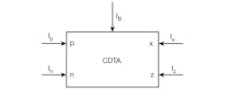
1. This simple diagram represents a basic symbol for a current differencing transconductance amplifier (CDTA).
The CDTA represents a synthesis of the well-known advantages of a current-differencing buffered amplifier (CDBA)2 and a multiple-output operation transconductance amplifier(OTA)3 to facilitate the implementation of current-mode analog signal processing. It also exhibits capability for electronic tuning by means of its transconductance gain, gm. As a result, CDTAs have been widely used in current-mode signal-processing circuits, such as inductance simulator circuits4-6 and sinuosoidal oscillator circuits,7-9 and is a promising choice for current-mode filters.10-19
CDTA-based biquad universal filters have undergone considerable study. For example, refs. 20 and 21 detail work on a CDTA-based Kerwin-Huelsman-Newcomb (KHN) current-model filter and a multiple-input, single-output universal filter, respectively. Both filters incorporate two CDTAs, two grounded capacitors, and simple structures. Reference 22 also reports on a CDTA-based universal filter which can be cascaded while simultaneously providing all standard filter functions. However, in spite of these reported filter circuits, research on nth-order CDTA-based filters has been inadequate.23-26
References 23 and 24 proposed two kinds of nth-order current-mode filters using CDBAs. These filters are realized with the aid of a signal-flow graph and employ too many passive components. Reference 25 details a CDTA-based nth-order lowpass filter with a simple structure and n grounded capacitors. It is based on the analysis of a signal-flow diagram. Reference 26 proposes a method for creating an nth-order circuit, in which a fourth-order bandpass filter is designed.
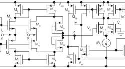
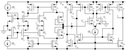
2. This circuit is a realization of a CMOS-based CDTA filter.
These design approaches suffer drawbacks, however. They can only realize nth-order single filter functions, such as a lowpass filter,25 and do not meet the requirements of a universal filter. These approaches employ circuit structures with single inputs to single outputs.23-26 When needing to change the filter function, the circuit’s topology must be changed simultaneously, not taking full advantage of the port characteristics and providing only limited filter flexibility. Another drawback is that these circuits are complicated and require many passive components; for example, the circuits in refs. 23 through 25 require external resistors and more CDTAs than the circuit of ref. 26.
Because of the shortcomings of these different universal filter design approaches, a new general synthesis method for CDTA-based resistorless nth-order current-mode universal filters was developed; it is based on mathematical analysis of transfer functions and signal-flow graphs. The circuit realization is obtained from a signal-flow graph, and the circuits developed from this approach feature a current-mode, multiple-input, single-output structure. By manipulating the amount and mode of joining the external current signals, a single circuit can provide lowpass, highpass, bandpass, band-stop, and all-pass filter functions without changing the topology.
The natural angular frequency of the filter, ω0, can be adjusted properly by means of current IB. The circuit configuration is simple: It contains n active components, n grounded capacitors, and no resistors, which is advantageous for IC fabrication. The required values of the passive elements can be found from the coefficients of the transfer function to be realized. Such a universal filter can be used in many applications, including in RF/microwave transmitters/receivers, in phase-locked-loop (PLL) frequency-modulation (FM) demodulators, in test instrumentation, and in wireless communications systems. It can also be used for an active filter in place of the surface-acoustic-wave (SAW) filters typically used in GSM systems.
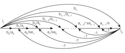
3. This is an nth-order equivalent signal flow graph for the universal filter.
The circuit symbol of the CDTA is shown in Fig. 1, where p and n are positive and negative current input terminals, z and x are current output terminals. Its current characteristics can be described by the matrix of Eq. 1:
where Vz = Iz * Zz; gm = the transconductance gain; and Zz = an external impedance connected at terminal z.
According to Eq. 1, the currents through terminal z follow the difference of the currents through terminals p and n (Ip – In), and flows from terminal z into an impedance Zz. The voltage drop at terminal z is transferred to a current at terminal x (Ix by means of transconductance gm, which is electronically controllable by an external bias current, IB.
Such a universal filter can be constructed using a number of techniques: a possible CMOS-based CDTA circuit suitable for IC fabrication is shown in Fig. 2.20 The transconductance stage can be copied in a circuit, so the number of x ports for the CDTA can be chosen as needed.
This file type includes high resolution graphics and schematics.
For the design of an nth-order universal filter, the transfer function can be written as Eq. 2:
where:
To present the feedback coefficient with units of gain and to simplify the design of the circuit, Eq. 3 can be modified, using the equivalent signal-flow graph shown in Fig. 3. According to the signal-flow graph, and using the Mason formula leading with the input variable, the output signal can be described by Eq. 4:
where I1, I2… In + 1 is the input variable with relationship to input signal Ii described by Eq. 5:
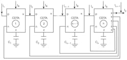
The system block diagram for Eq. 4 is shown in Fig. 4. Using Fig. 4, the proposed CDTA-based nth-order current-mode universal filter can be obtained as shown in Fig. 5. By routine analysis, the single-output-current function realized by this circuit configuration is:
where:
τ0 = gmn/Cn,
τ1
= gmngm(n - 1)/CnCn - 1, . . .
That is:
and gmi is the transconductance gain parameter of the ith CDTA.
4. This is an nth-order functional equivalent circuit block diagram for the universal filter.
From Eq. 6, through a rational changing of the amount and mode of joining the external current signals, it is possible to derive the filter function in the following five ways:
1) If I1 = Iin and I2 = … In = In + 1 = 0, the lowpass filter response can be realized.
2) When n is an even number, if:
In/2 = Iin, and the other input currents are zero, or when n is an odd number, if In - 1/2 = Iin or:
I(n + 1)/2 = Iin and the other input currents are zero, a bandpass filter response can be realized.
3) If I(n + 1) = Iin and I1= … = In = - Iin, a highpass filter response can be realized.
4) If I(n - 1)/2 = Iin and 2 = … = In = - Iin, and I1 = 0, a bandstop filter response can be realized.
5) When n is an even number, if In + 1 = Iin,
In = -2Iin,
In - 1 = 0,
In - 2 = -2Iin,
In - 3 = 0, . . . , I2 = -2Iin,
In - 1 = 0, or when n is an odd number, if:
In + 1 = Iin,
In = -2Iin,
In - 1 = 0,
In - 2 = -2Iin,
In - 3 = 0, . . . , I2 = 0, and
I1 = -2Iin,
an all-pass filter response can be realized.
5. This is a proposed CDTA-based nth-order current-mode universal filter.
From Eqs. 6, 7, and 8, when calculating the required component parameters, if all gm1 values are known (according to the filter transfer function), the value of capacitance Cn can be found from τ0 and then the value of Cn - 1 can be found from τ0, τ1. The other values can then be confirmed, and so forth, since it is fairly straightforward to find the values of passive elements from the coefficients of the transfer function to be realized. It is also apparent that the angular frequency of the filter, &omega0, can be adjusted properly by adjusting current IB.
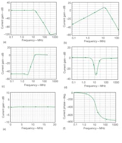
6. These frequency responses show the different proposed filter functions: (a) lowpass, (b) bandpass, (c) highpass, (d) bandstop, (e) all-pass frequency response, and (f) all-pass phase response.
To verify this theoretical analysis, a simulation was performed in PSpice, for a current-mode fourth-order Butterworth filter using the CMOS-based CDTA circuit of Fig. 2. The filter was modeled in PSPICE with 0.5-μm CMOS parameters, available upon request from the authors. The cutoff frequency of the fourth-order Butterworth filter is 13 MHz,27
The filter has a transfer function denominator polynomial of D(s) = s4 + 2.14 × 10⁷ + 2.292 × 10¹² s2 + 1.437 × 10¹⁷ s + 4.506 × 10²¹. The CDTA element in this case has a bandwidth of approximately 420 MHz, and the circuit is supplied with symmetrical voltages of ±2.5 VDC. The external bias currents are IB1 =
IB2 = 85 μA, IB3 = 200 μA, and the transconductance gain, gm1, is 457.83 μS. One of these CDTAs is modified from the circuit in Fig. 2 and is chosen with five x ports. It is easy to obtain the value Ci from the above parameters: C1 = 15 pF, C2 = 7.3 pF, C3 = 4.27 pF, and C4 = 2.14 pF. Figure 6 shows the simulation results, with theoretical test and computer simulation results in good agreement.
Jun Xu, Master’s Degree Candidate
Unit 95316 of the People’s Liberation Army, Guangzhou 510900, People’s Republic of China; e-mail: [email protected].
Chunhua Wang, Professor and Doctoral Supervisor
College of Information Science and Engineering, Hunan University, Changsha 410082, People’s Republic of China, e-mail: [email protected].
This file type includes high resolution graphics and schematics.
Acknowledgments
The authors would like to thank the National Natural Science Foundation of China for financially supporting this research under grant number 61274020, as well as the Open Fund Project of the Key Laboratory of Hunan University in the People’s Republic of China (under grant number 12K011) and the Hunan Provincial Natural Science Foundation of China (grant number 11JJ6055) for their support. The authors are also thankful to the editor and anonymous reviewers for their valuable comments and helpful suggestions, which have substantially improved the quality of the final article.
References
1.D.Biolek, “CDTA-Building block for current-mode analog signal processing,” in Proceeding of the ECCTD’03, Krakow,Poland,Vol. 3, 2003, pp. 397-400.
2. C. Acar and S. Ozoguz, “A new versatile building block: current differencing buffered amplifier suitable for analog signal processing filters,”Microelectronics Journal, Vol. 30, 1999, pp. 157-160.
3. Y.S. Zhao, Y.Q. Zhou, and P. Wang, “Electronic circuit of current-mode,” Tianjing University Press, Tianjing, People’s Republic of China, 2001.
4. W. Jaikla and M. Siripruchyanan, “Current controlled CDTA (CCCDTA) based novel floating and grounded inductance simulators,”Communications and Information Technologies, Vol. 3, 2006, pp. 348-351.
5. M. Siripruchyanun and W. Jaikla, “CMOS current-controlled current differencing transconductance amplifier and applications to analog signal processing,”International Journal of Electronic Communications (AEÜ), Vol. 62, 2008, pp. 277-287.
6. M. Siripruchyanun and W. Jaikla, “Current-controlled current differencing transconductance amplifier and applications in continuous-time signal processing circuits,”Analog Integrated Circuits and Signal Processing, Vol. 61, 2009, pp. 247-257.
7. W. Tangsrirat, et al., “Current-mode multiphase sinusoidal oscillator using CDTA-based allpass sections,”International Journal of Electronic Communications, doi: 10.1016/j.aeue.2008.05.001,2008.
8. A.U. Keskin and D. Biolek, “Current mode quadrature oscillator using current-differencing transconductance amplifiers (CDTA),”IEEE Proceedings—Circuits, Devices, and Systems, Vol. 3, 2006, pp. 248-252.
9. L. Abhirup, “Novel voltage/current-mode quadrature oscillator using current-differencing transconductance amplifier,”Analog Integrated Circuits and Signal Processing, Vol. 61, 2009, pp. 199-203.
10. M. Siripruchyanun and W. Jaikla, “Electronically controllable current-mode universal biquad filter using single DO-CCCDTA,”Circuits and Systems Signal Processing, Vol. 27, 2008, pp. 113-122.
11. N.A. Shah, M. Quadri, and S.Z. Iqbal, “CDTA based universal transadmittance filter,” Analog Integrated Circuits and Signal Processing, Vol. 52, 2007, pp. 65–69.
12. W. Tanjaroen and W. Tangsrirat, “Current-mode second-order notch filter using CDTA-based allpass sections,”SICE Annual Conference, 2008, pp.1143-1146.
13. W. Tanjaroen, T. Dumawipata, and W. Tangsrirat, “TISO cascadable current-mode multifunction filter employing current differencing transconductance amplifiers,”SICE-ICASE International Joint Conference, 2006, pp. 5703-5706.
14. W. Tanjaroen and W. Tangsrirat, “Resistorless current-mode first-order allpass filter using CDTAs,”Electrical Engineering, Electronics, Computer, Telecommunications, and Information Technology, Vol. 2, 2008, pp. 721-724.
15. W. Tangsrirat, T. Pukkalanun, and W. Surakampontorn, “Resistorless realization of current-mode first-order allpass filter using current differencing transconductance amplifiers,”Microelectronics Journal, Vol. 41,2010, pp. 178-183.
16. A. Uygur and H. Kuntman, “Seventh-order elliptic video filter with 0.1 dB pass band ripple employing CMOS CDTAs,”International Journal of Electronics and Communications, Vol. 61, 2007, pp. 320-328.
17. D. Prasad, et al., “Universal current-mode biquad filter using dual output current-differencing transconductance amplifier,”International Journal of Electronics and Communications, doi: 10.1016/j.aeue.2008.02.012.
18. W. Tangsrirat and T. Pukkalanun, “Structural generation of two integrator loop filters using CDTAs and grounded capacitors,”International Journal of Circuit Theory and Applications, Vol. 39, 2011, pp. 31–45.
19. D. Prasad, D.R. Bhaskar, and A. K.Singh, “Multi-function biquad using single current-differencing transconductance amplifier,”Analog Integrated Circuits and Signal Processing, Vol. 61, 2009, pp. 309-313.
20. A. U. Keskin, D. Biolek, E. Hancioglu, and V. Biolkova, “Current-mode KHN filter employing current-differencing transconductance amplifiers,”International Journal of Electronic Communications, Vol. 60, 2006, pp. 443-446.
21. W. Tangsrirat, T. Dumawipata, and W. Surakampontorn, “Multiple-input single-output current-mode multifunction filter using current-differencing transconductance amplifiers,”International Journal of Electronic Communications (AEÜ), Vol. 61, 2007, pp. 209-214.
22. T. Dumawipata, W. Tangsrirat, and W. Surakampontorn, “Cascadable current-mode multifunction filter with two inputs and three outputs using CDTAs,” Information, Communications, and Signal Processing, 2007 6th International Conference, Vol. 4, 2007, pp. 10-13.
23. C. Acar and S. Ozuguz, “Nth-order current transfer function synthesis using current differencing buffered amplifier: signal-flow graph approach,”Microelectronics Journal, Vol. 31, 2000, pp. 49-53.
24. M. Koksal and M. Sagbas, “A versatile signal flow graph realization of a general transfer function by using CDBA,” International Journal on Electronic Communications, Vol. 61,2007, pp. 35-42.
25. A. Bekri and F. Anday, “Nth-order lowpass filter employing current differencing transconductance amplifiers,”in Proceedings of the 2005 European Conference on Circuit Theory and Design, Cork, Ireland, Vol. 2, 2005, pp. 193-196.
26. T. Dostal, V. Smejkal, and J. Slezak, “Realization of arbitrary transfer current characteristic using transconductors CDTA,”2008 18th International Conference on Radioelektronika, Vol. 4, 2008, pp. 24-25.
27. J.L. Zhen, Q.H. Ying, and W. L.Yang, Signals and Systems, High Education Press, Beijing, People’s Republic of China, 2000.
