This file type includes high resolution graphics and schematics when applicable.
Before electronic control and actuation, mechanically actuated RF switches were used to re-route RF energy to different subsystems. Out of necessity, these switches were often custom, expensive, slow, and prone to failure. But they could handle significant amounts of RF energy.
Maturation of electronic actuation and control led to RF switching with faster, more reliable electromechanical switches. Nonetheless, electrically actuated switches still were limited in their ability to handle high frequencies, due to limits in the mechanical tolerances of fabrication technology. In the 1950s, solid-state switches emerged when it was found that semiconductor materials could be used to channel RF energy. These switches were notably smaller and faster and could operate at much higher frequencies.
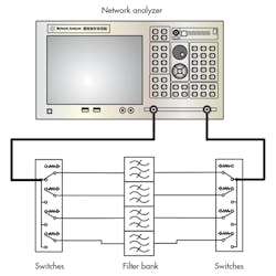
In the years since, a growing number of applications have benefited from higher-performance, smaller, and more integrated RF switches (Fig. 1). Such demand has driven advances in solid-state and electromechanical materials and fabrication technologies. The latest switches from these two groups are reaching ever-smaller sizes, greater switching speeds, lower costs, and higher frequencies.
1. Electromechanical Switches
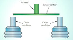
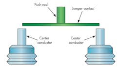
As the successors of purely mechanical switches, electromechanical switches use electrical actuators to make a physical connection between RF-path conductors. These RF paths can be waveguides, or coaxial or stripline transmission lines. The electrical actuators are often small solenoids connected to insulating plungers (Fig. 2). When force is applied to a metallic member, the RF paths are connected.
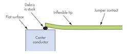
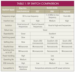
High-performance electromechanical RF switches, which benefit from enhanced machining technologies, can reach into the millimeter-wave frequencies with very high isolation and very low insertion loss. Electromechanical switches also excel in the areas of high-power handling, linearity, and low harmonics. In addition, they exhibit no compression region. As a function of the electrical actuation and mechanical connection design, electromechanical switches are limited to tens of milliseconds in the highest-precision designs. Any contaminants in the electromechanical switch can also reduce device performance (Fig. 3).
2. RF Microelectromechanical-Systems (MEMS) Switches
Technologies that can create extremely small and high-tolerance mechanical features have been developed to overcome the limitations of traditional machining. Known as microelectromechanical systems (MEMS), they use processing that’s similar to semiconductor device fabrication. MEMS devices can be made smaller, lighter, and more precise with the potential to be integrated alongside control electronics.
These new techniques have led to microwave and millimeter-wave devices that are less prone to mechanical wear, vibration, and repeatability issues. They also suffer from less parasitic effects, making them a more ideal solution for millimeter-wave applications. The two most common typologies of RF MEMS switches are ohmic and capacitive contact switches.
Using capacitive contact typology, MEMS fabrication techniques have been used to develop commercially available switches that operate into the low millimeter waves. MEMS switches are much faster than traditionally manufactured RF switches, but have yet to reach the speeds of PIN-diode or even FET-based switches. For some applications, however, the cost reductions and power savings derived from RF MEMS switches make them a viable alternative.
Ohmic switches have previously been seen as less reliable and more costly than capacitive contact switches, hindering their adoption. But, enhanced RF MEMS fabrication capability has made ohmic contact switches become more realizable. Instituting these new fabrication capabilities helps push the ohmic contact typology toward lower insertion loss and greater isolation and linearity.
3. Field-Effect-Transistor (FET) Switches
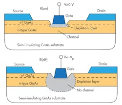
Dominating the realms of FET switches is the heterostructure FET (HFET) or high-electron-mobility transistor (HEMT) using gallium arsenide (GaAs) and aluminum gallium arsenide (AlGaAs). The heterostructure technology increases the FET switch’s upper-frequency response (Fig. 4).
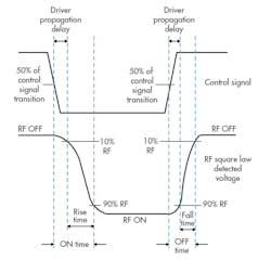
FET-based switches exhibit high isolation at low frequencies and operation down to direct current (dc). When the transistor is in reverse-biased condition, resistance from drain to source is extremely high. At high frequencies, the parasitic capacitance between the drain and source degrades the switches’ isolation. To note, the FET’s parasitic capacitances lead to switching speeds in the tens of nanoseconds. Yet hundreds of microseconds of additional gate lag prevent faster switching.
The signal path or on resistance of a FET switch is generally high enough to reduce insertion-loss performance compared to other switch technologies. High on resistance tends to negatively impact insertion loss. In addition, the voltage-controlled on resistance is very stable and repeatable. Such voltage control leads to low current consumption for switching, which in turn fosters low-power operation.
Advances in silicon-on-insulator (SOI) technology have produced FETs that perform at higher frequencies while retaining low cost and silicon-based CMOS integration. SOI exceeds traditional GaAs technology in terms of power handling and electrostatic-discharge (ESD) survivability. For example, SOI-based switches can integrate control electronics and memory on the same substrate as the FETs. Recently, RF SOI switches reached performance levels comparable to that of GaAs-based switches, leading to RF SOI’s extensive use in high-volume applications like cellular handsets.
4. Solid-State Switches: PIN-Diode Switches
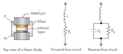
Unlike FET switches, a PIN diode acts as a variable resistance with a low on resistance (usually below 1 {greek capital OHM}) and a high off state resistance (generally in the tens of kilohms). The intrinsic region’s thickness dictates the attenuation of the lower frequencies and the amount of power necessary to forward-bias the diode. Variations in the intrinsic layer thickness can change the lower frequency capability of the diode from tens of kilohertz to tens of megahertz at the lower limit.
The characteristics of the semiconductors used—silicon (Si), GaAs, AlGaAs, and now gallium nitride (GaN)—dictate the frequency and power-handling capability of a switch constructed from PIN-diode components. A PIN-diode switch’s diodes also must be dc-biased, which requires capacitive, inductive, and RF choke components. The circuit typology—either series or shunt—dictates the isolation, insertion loss, and bandwidth operation of the PIN diode switch.
Series PIN-diode switches often display low isolation with wide bandwidths, which are only limited by the dc blocking capacitors and biasing inductors. The bandwidths of shunt PIN diodes, on the other hand, are limited by the transmission lines used to interconnect the common junction to each PIN diode.
The shunt typology generally exhibits much higher isolation, though, which requires a tradeoff of insertion loss. Often, hybrid typologies are used to deliver a balance of isolation, bandwidth, and insertion loss depending on the application.
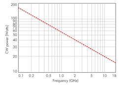
PIN-diode switches are generally a low-cost RF/microwave switching option ranging from milliwatts to tens of kilowatts of average power handling, depending on size. As the frequency increases, the average power-handling capability of these switches will decrease with size. PIN-diode switches differentiate themselves from FET-based switches in terms of their extremely fast switching speed, which can reach nanosecond transition times.
5. Hybrid Solid-State Switches
PIN-diode and FET switches have intrinsic benefits and drawbacks. Yet hybrid combinations of both technologies can potentially mitigate each technology’s drawbacks. Such hybrid approaches are possible with certain semiconductors, and particular topologies will be able to leverage both bandwidth and isolation advantages.
For example, a hybrid switch combines series FET devices and shunt PIN-diode devices (Fig. 5). As a result, the PIN-diode switch’s frequency response lowers to dc while the high-end frequency isolation response of the FET-based switches gets a boost.
As shunt PIN diodes are used, there will be current draw in order to bias this diodes. This leads to slightly less power efficiency than with purely FET typologies. Additionally, the RF paths and biasing should be isolated. Otherwise, there is the potential for RF leakage into the DC biasing path.
6. Switch Typologies/Configurations
There are several different switch topologies and configurations. Failsafe and latching are the most common (Fig. 6). Failsafe switches will return to the default state after the control signal is removed. Generally, solid-state switches are failsafe or normally open switches. The default position of the normally open switches is disconnected. In contrast, latching switches maintain the position that was last set after the control signals aren’t present.
Aside from types of switches, RF/microwave switches will employ one of three main configuration. Single-pole, double-throw (SPDT) switches are used to route an RF signal input to two outputs or two outputs to a single input. Double-pole, double-throw (DPDT), or transfer switches, redirect the RF signal from two inputs and two outputs. And multiport switches, which have several output/input positions, redirect an RF signal from one input to more than three outputs or vice versa. These switch configurations can also be a sub-component of larger switch matrices to form a configurable RF path.
This file type includes high resolution graphics and schematics when applicable.
Resources:
Power Handling Capability of Electromechanical Switches
Understanding RF/Microwave Solid State Switches and their Applications
Switching Solutions For Research and Development, Design Validation, Manufacturing
Microwave Switches: Application Notes
Configuring an Optimal RF/Microwave Switch System
Applications for the HSMP-3890 Surface Mount Switching PIN Diode
