This file type includes high-resolution graphics and schematics when applicable.
Microwave packaging is a term that covers a lot of ground (and relies on a reliable ground plane), and includes many configurations and material compositions. Such packages range in size from microscopic to cabinet-sized for system assemblies. But whatever the size or type, all microwave packages are designed to protect the electronic devices, components, and circuits within them. Depending on the materials and construction, they may be rated for different levels of temperature, humidity, vibration, shock, and input power. What follows is a brief glimpse at some of the different package types used across the RF/microwave industry.
Increased integration has been an ongoing goal for RF/microwave package developers to support the mass adoption of high-frequency technology in products like cellular telephones and wireless local-area networks (WLANs). It is safe to say that wireless technology brought high-frequency packaging into a more integrated realm. That should continue as RF, microwave, and even millimeter-wave technologies merge with the Internet via the fifth generation (5G) of wireless networks and such applications as wearable devices and the Internet of Things (IoT) devices. These applications are expected to increase the use of system-in-package (SiP) and system-on-chip (SoC) devices in order to integrate radio and control circuitry within a single, compact housing.
SoC and SiP devices consist of different package configurations, such as two-dimensional (2D) and three-dimensional (3D) versions. In the former, semiconductor devices are placed in a horizontal layout while in the latter, to save space, devices are mounted and stacked vertically, typically on the layers of a multilayer printed-circuit board (PCB). Devices within a SiP are usually interconnected internally by flip-chip or wire-bond approaches.
Multichip modules (MCMs) follow a similar integration approach as SiPs and SoCs, with multiple discrete devices or ICs contained within a single package. One difference between an MCM and SiP, however, is that an MCM provides package pin connections for the difference devices contained within, rather than the system-level control of an SiP or SoC. This makes it possible to provide biasing for individual components, such as a discrete power transistor or an active mixer.
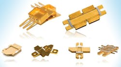
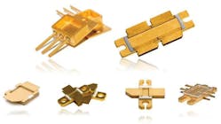
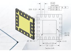
These higher levels of packaged integration are driven by requirements for smaller size and less power consumption (Figs. 1 and 2). While packaging approaches such as SoCs, SiPs, and MCMs support miniaturization, a price is paid for that small size: Integrating multiple active and passive components within a single package tends to result in reduced production yields, since any one defective component in the module will cause the entire module to fail.
Tough Packaging Tasks
Perhaps one of the more difficult RF/microwave devices to package is the high-power discrete transistor or high-power monolithic-microwave-integrated-circuit (MMIC) amplifier. Though physically small, it is a large source of heat. In addition to providing an effective thermal path from the active device to outside circuitry or a heat sink, the packaging materials must also offer low-loss transmission paths for input and output signals and, in some cases, operate effectively with high voltages.
With the increasingly widespread use of high-power-density devices such as gallium-nitride (GaN) transistors, thermal management in packaging is becoming as great a concern as electrical performance. Ideally, a GaN device would turn all applied electrical energy into electromagnetic (EM) energy, and very little heat would be dissipated. But modern power transistors and MMIC amplifiers are not capable of perfect power-added efficiency (PAE) and a considerably amount of bias energy converts into heat, which must be dissipated efficiently to ensure the long-term reliability of the device and surrounding circuitry.
Power transistor packages have customarily incorporated ceramic frames with conductive metal grounds and conductors, such as copper (Cu). The main problem in packaging a device that may generate a large amount of heat in a small space is the differences in the coefficient of thermal expansion (CTE), such as the ceramic, Cu, and semiconductor die itself. When they don’t match closely enough, the materials will expand and contract with temperature at different rates, causing stress and cracks in the ceramic or copper conductors.
High-power transistor packages have traditionally provided reliable thermal paths, typically by means of robust flange-mount packages (Fig. 1, again). While thermally efficient, such packages are large and expensive, driving many semiconductor manufacturers to search for more cost-effective ways of packaging high-power RF/microwave transistors and MMICs
Kyocera, a company long associated with high-quality device packaging, has done extensive research on different materials for heat sinks used in high-power packaged transistors, for the purpose of finding a cost-effective material with efficient thermal dissipation. Cu heat sinks are estimated to have 40 to 50% reduction in thermal resistance compared to more exotic (more expensive) copper-tungsten (CuW) materials. Cu, the lowest-cost heat-sink material, is readily available from multiple sources to reduce cost. Any material with enhanced thermal properties compared to copper will be more expensive, such as copper silicon carbide (CuSiC), Cu diamond, and Cu graphite.
As the firm found, copper laminates could serve in place of the more exotic CuW base and heat sink materials in high-power packages. As with CuW, the copper laminates supported high-temperature brazing to alumina for fabrication of ceramic packages, with a significant improvement in thermal resistance and potential cost reduction compared to CuW. In addition, CuW has a much higher modulus of elasticity (is much stiffer) than copper, allowing for some greater tolerances in the assembly and manufacturing processes.
However, in the Kyocera studies, it was found that copper and CuW differed somewhat in terms of surface defects, which could impact the thermal flow from an active device to the heat sink. CuW is a machined or ground substance with very even and consistent surface, while rolled copper or copper laminates have very uneven surfaces and are subject to voids underneath a semiconductor die mounted on their surface. Such voids are interruptions in the thermal path and can become hotspots at high power levels and temperatures.
Searching Beyond Ceramics
But is there some alternative to ceramic materials, such as alumina and low-temperature cofired ceramic (LTCC) for high-power RF/microwave device packages? With the widespread adoption of GaN as the high-power RF/microwave semiconductor substrate of choice, and with higher-power applications, such as radar systems, no longer the exclusive domain of military systems, the need for lower-cost power RF/microwave device packaging is apparent.
Package and semiconductor developers have long considered alternatives to ceramic package frames, including organic laminates and plastic materials. In fact, several firms have introduced high-power devices in packages with plastic frames, both for continuous-wave (CW) and pulsed applications.
A growing number of higher-power GaN devices are becoming available in low-cost plastic packages as well. Two years ago, at the International Microwave Symposium (IMS), Cree/Wolfspeed introduced a line of GaN discrete transistors capable of operating at frequencies to 3.8 GHz in plastic packages, including a 300-W model. The +50-V dc transistors operate across multiple cellular communications bands with 65% efficiency at saturated output-power levels. The plastic packages not only provide effective thermal management, but they help lower cost and reduce the weight of each device.
Cree was not alone in pursuit of plastic-packaged high-power GaN devices, as witnessed by the plastic-encased transistors or amplifiers made available from MACOM, Qorvo, and NXP. In MACOM’s case, the MAGX family of devices, based on the firm’s GaN-on-silicon-carbide (GaN-on-SiC) semiconductor process, is housed in lightweight plastic packages. Considerably lighter than their ceramic counterparts, these packages employ advanced heat-sink approaches and die-attachment techniques to achieve less than +115°C average junction temperature (with an +80°C base plate) for a pulsed output power of 93 W. The input pulses have a 1000-µs pulse width and 10% duty cycle.
The plastic transistors, designed for use at +50 V dc, come in standard 3- × 6-mm dual-flat-no-lead (DFN) packaging. They can be mounted on PCBs by means of ground/thermal arrays and be reliably operated at temperatures to +200°C or higher. In fact, the plastic-packaged devices were lifetime-tested and projected to have high reliability for 100 years when operating at +218°C. They are suitable replacements for power transistors in much larger and costlier flanged metal packages.
Just one year ago, NXP/Freescale introduced its RF5011N, a GaN-on-SiC transistor in a plastic package for use at frequencies to 3 GHz. Designed for a +28-V dc supply, it provides 10-W output power with 10-dB gain. The transistor is surrounded by the firm’s OM-270-8 plastic packaging and uses advanced die-attach technology to achieve outstanding thermal-resistance characteristics even without the ceramic materials. The firm’s higher-power 125-W (from a +50-V dc supply) model RF5015N also comes in the plastic package.
Reaching Higher
As RF/microwave package developers learn how to handle high power levels and heat with lower-cost materials, similar challenges await designers of packaging for millimeter-wave devices. This especially comes to light with the accelerated growth in automotive radar-based vehicle safety systems and the expected rapid spread of millimeter-wave frequencies for 5G, once wireless standards are established for that next-generation cellular system.
As at lower frequencies, miniature surface-mount (SMT) packaging will be needed for lower-power active and passive components and more robust packaging for devices and components at higher power levels. At the same time, they must also support the transmission of signal frequencies of 30 GHz and beyond.
Organizations such as the University of California at Davis, known for its work at millimeter-wave frequencies, have devoted a great deal of research to the development of SMT and power packages for millimeter-wave applications. Much of those studies have focused on the development of liquid-crystal polymers (LCPs) for multilayer packages and modules at microwave and millimeter-wave frequencies. The materials feature low loss (for microstrip lines) and low moisture absorption for projected IoT applications in industrial settings, such as oil fields and down wells.
Many of the mechanical attributes, such as CTE, are closely matched to those of Kapton. LCP exhibits stable dielectric constant even in humid environments, and can be used to form organic millimeter-wave SMT packages. In measurements of prototypes, and in simulations with software tools like ANSYS’s High-Frequency Structure Simulator (HFSS), the organic material shows great promise as a hermetic package building material for use to 50 GHz and beyond.
Within the industry, of course, a number of companies have long addressed the need for millimeter-wave packaging, with companies such as StratEdge Corp. and Palomar Technologies having developed package solutions for high-power and high-frequency applications. These packages incorporate many traditional conductor and ceramic dielectric materials, and they provide the performance required through 60 GHz and beyond. The next step in package evolution will be to provide different types of lower-cost packages for the likely heightened demand for millimeter-wave components.
Looking for parts? Go to SourceESB.


