Download the PDF of this article.
Digital television broadcast standards employ various forms of amplitude-modulated (AM) signals with suppressed sidebands to reduce emissions and interference. An example is the Advanced Television Systems Committee (ATSC) 8-level vestigial sideband (8VSB) American standard for digital broadcast television in the United States, as well as its analog predecessor, the National Television System Committee (NTSC) standard. High-power high-definition-television (HDTV) transmitters require stringent emission masks to reduce sidebands and to achieve spectrally pure signals.
To accomplish this, many 8VSB modulators have incorporated surface-acoustic-wave (SAW) filters for high sideband attenuation. Unfortunately, such filters are often plagued by excessive passband amplitude ripple, high passband insertion loss, and high cost. However, the use of digital modulation techniques, such as field-programmable gate arrays (FPGAs) and digital signal processors (DSPs), has made it possible to implement digital television modulators that overcome the limitations of SAW filters. Through the use of DSP techniques, it is possible to generate both analog AM-VSB and digital 8VSB television signals with a single platform.
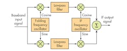
A modulation method known as Weaver modulation has been used to generate single sideband (SSB) signals with arbitrary sideband shape.1-4 Because the approach requires two precisely matched filters and signal paths, it has rarely been implemented in analog circuitry. However, such matching is routinely possible with DSP circuitry. Figure 1 depicts a Weaver modulator, which begins by multiplying the modulating signal with a pair of quadrature phased sinusoidal signals.5, 6 When generating a SSB signal, the frequency of the sinusoidal is one-half the modulation bandwidth.
1. This block diagram shows the components and architecture of a Weaver modulator.
The frequency of these two signals is called the folding frequency, and the signal multiplication produces a pair of orthogonal baseband signals. A lowpass filter following each modulator restricts the bandwidth of each output to one-half of the bandwidth of the original modulating signal. At this point, the modulating signal has been folded in such a way that the folding frequency is translated to DC, while both the upper and lower band edges are translated to the highest frequencies in the folded spectrum.
The two baseband signals are then applied to a quadrature mixer. If the quadrature phases are accurate; if the two lowpass filters are matched; and if the gain, phase, and delay of the two signal paths are matched, the sum of the two signal paths is a SSB signal.
Discrete analytic signals yield a null in Fourier transform values for frequencies of –π ≤ ω < 0. The Hilbert transform is a mathematical method for describing the analytic signal sa(n) (sometimes known as the complex envelope) of a real-valued baseband signal s(n) as:
sa(n) = s(n) + jH[s(n)],
where H[s(n)] is the Hilbert transform of baseband signal s(n).7 The definition of this linear operator has the convolution form of H[s(n)] = s(n) * h(k). This transformation can be implemented as the output of a linear time-invariant system with input s(n), and an impulse response represented in the form h(k) = 2sin2(πk/2)/πk. The Hilbert transform has the effect of shifting the frequency components –π ≤ w < 0 of s(n) by 90 deg., as well as the frequency components 0 ≤ ω < π by –90 deg. This occurs because of the frequency response behavior of the Hilbert transform linear system: F{h(k)} = H(ω) = –jsgn(ω) where H(ω) is the discrete-time Fourier transform of h(k).6
The lower sideband from an AM signal is produced due to the presence of the negative part of the spectrum, and this must be eliminated. These negative frequencies may be cancelled by applying the modulating baseband signal in a system with suitable frequency response, where the transmitting bandwidth is represented by ωm. To obtain the impulse response for this system, consider a discrete-time Fourier transform (DTFT). Let x(n) be a real-valued signal with a DTFT defined by Eq. 1:
According to the symmetry property, if x(n) is real, X(ω) is a conjugated symmetric, which satisfies all of the equations for even and odd symmetry with the relationship expressed by Eq. 2:
The desired system cannot be achieved using a real-valued impulse response, since symmetry around the zero frequency makes it impossible to discriminate positive and negative frequencies. To generate the desired system response, it is necessary to use a complex-valued impulse response, in the process departing from the frequency shifting property of the DTFT function. This can be done by using a lowpass filter with cutoff frequency of ωm/2 and a real-valued impulse response hr(k) with N taps and 0 ≤ k ≤ N – 1.
As a direct consequence, the desired frequency response can be obtained by multiplying the hr(k) response by the complex function with frequency ωm/2, wm/2, resulting in a complex-valued impulse response hc(k), in the form of Eq. 3:
Thus, Hr(ω) presents a passband from –ωm/2 to +ωm/2, while function Hc(ω) provides a passband from 0 to ωm due to the ωm/2 shifting. It can be proven that there is an optimum initial phase value ϕ for the complex function that will avoid phase distortion of the complex envelope to be generated.2 The initial phase ϕ is used to guarantee an optimization criterion where both real and imaginary parts of the complex impulse response hc(k) must present an even and odd symmetry, respectively.7
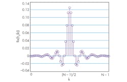
2. The plot shows the real part of the impulse response.
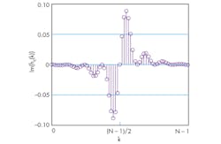
Following this criterion, the complex function at the instant k = (N – 1)/2, which corresponds to the hr(k) symmetry point, must be null. This results in an initial phase to applied in Eq. 3, where ϕ = –(1/2)[(ωm/2) • (N – 1)]. Figures 2 and 3 illustrate both real and imaginary parts of hc(k), with the phase correction. If a signal s(n) is applied into this complex filter, the output is a band-limited analytic signal, sa.
3. This is a visualization of the imaginary part of the impulse response.
Digital television 8VSB modulation is considered to be a vestigial-sideband signal because actual filters differ from ideal ones, so that the vestigial sideband corresponds to the filter rolloff. Ideally, this system could be called 8-SSB. But in analog broadcast television systems like NTSC, a large amount of the sideband is intentionally transmitted. As a result, what was shown earlier for SSB signals can be generalized for AM-VSB signals.
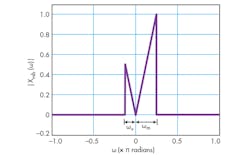
4. This is a representation of an AM-VSB signal.
This can be done by considering ωm as the bandwidth from one sideband and ωv as the bandwidth from the vestigial sideband, as shown in Fig. 4. If hr-vsb(k) represents the real impulse response of a lowpass filter with cutoff frequency equal to (ωm + ωv)/2, with 0 ≤ k ≤ (N – 1), then a baseband signal that describes the AM-VSB channel can be generated by filter having the complex impulse response hr – vsb(k) which is defined by Eq. 4:
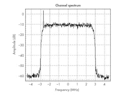
By performing a comparative study between the Weaver method and the complex filtering method proposed here using an 8-VSB modulator implementation, almost no difference exists in performance, as shown in Fig. 5.8 At this measurement, the lower sideband had been attenuated by 50 dB due to the orthogonal phase relationship between both baseband signals. Analysis of the channel spectrum generated by the complex filter method reveals no differences from previous modulation methods.
5. The plot shows the 8VSB spectrum for both signal generation methods
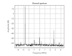
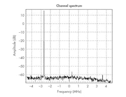
However, if a single symbol is transmitted continuously, which means transmitting a pure carrier, differences will appear in terms of in-channel spurious content. This can be seen in the measurements presented in Figs. 6 and 7. By using the Quartz II programming platform to implement the inside the FPGAs, Fig. 8 presents the architecture designed for all experimental measurements made over the modulator block for modern HDTV transmission systems.
6. This is a representation of the carrier resulting from the Weaver filtering method.
The FCC has mandated a period which ATSC and NTSC signals will be multicast. Transmission equipment that is suitable for both systems will provide the greatest degree of flexibility for the broadcaster. Quite possibly, the original, complex filtering approach presented here provides the flexibility needed to apply DSP techniques to modern broadcast television systems.
7. This is a representation of the carrier resulting from the complex filtering method.
8. The photograph shows the Quartz II programming platform used to validate the complex filtering approach for AM-VSB signal modulation.
Acknowledgments
The authors wish to thank the National Institute of Telecommunication, INATEL, Santa Rita do Sapucai, MG; Department of Electrical Engineering, DEE, UFSCar; Foundation of Research, FAPESP, São Paulo, SP, processes: 2006/01655-7, 2013/23431-7; all located in Brazil, and to Keysight Technologies for its assistance with the measurements.
Henry Douglas Rodrigues, Master of Science
National Institute of Telecommunications, INATEL, Santa Rita do Sapucai, Minas Gerais, Brazil
Jose de Souza Lima, Master of Science
Lima Construcoes e Projetos S/A, Santa Rita do Sapucai, Minas Gerais, Brazil; e-mail: [email protected]
Mauricio Silveira, Visiting Professor
DEE, UFSCar
Research Collaborator
DECOM, FEEC, UNICAMPUFSCar, Sᾶo Carlos, Sᾶo Paulo, Brazil
References
1. H.D. Rodrigues, M. Silveira, M.P.S. Silva, A.A. Mello, and J.S. Lima, “Uma Eficiente Abordagem para a Numérica Linearização de Amplificadores de Potência,” Revista Eletrônica do IEEE América Latina, Section 09, June 2004.
2. H.D. Rodrigues, M. Silveira, M.P.S. Silva, A.A. Mello, and J.S. Lima, “A New Numerical Approach in the Linear Analysis of RF Amplifiers,” IEEE Microwave Theory & Techniques Symposium (MTT-S), 2003, 33rd European Microwave Conference, Munich, Germany.
3. H.D. Rodrigues, M. Silveira, M.P.S. Silva, A.A. Mello, and J.S. Lima, “Adaptive Digital Pre-Distortion to Reduce the Power Amplifier Nonlinearity,” IEEE APS-URSI 2003, Columbus, OH, 2003.
4. H.D. Rodrigues, M. Silveira, A.A. Mello, J.S. Lima, and W.N. Pereira, “Transmitter Linearization Using Digital Pre-Distortion,” IEEE APS-URSI 2002, San Antonio, TX, 2002.
5. D.L. Hershberger, “Architecture of a DSP based Dual-Mode ATSC/NTSC Television Exciter and Transmitter,” www.broadcastpapers.com.
6. D.K. Weaver, “A third method of generation and detection of single-side band signals,” Proceedings of the IRE, Vol. 44, December 1956, pp. 1703-1705.
7. H.D. Rodrigues, M. Silveira, J.S. Lima, and B. A. Pereira, “Implementation of an AM-VSB Modulator using the Hilbert Transform,” IEEE APS-URSI 2004, Monterey, CA, 2004.
8. H.D. Rodrigues and M. Silveira, “Generation and Analysis of Vestigial Side Band Signals,” IEEE APMC 2005, Suzhou, China, 2005.

