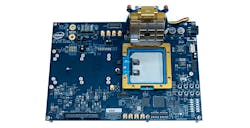
Taking advantage of the speed of light is one of the goals of the Photonics in the Package for Extreme Scalability (PIPES) program managed by the Defense Advanced Research Projects Agency (DARPA). Rather than building electronic systems using integrated circuits (ICs) interconnected by electrical systems, the PIPES program is seeking ICs that communicate with each other using photons or optical signals.
To help reach that goal, DARPA has recruited researchers from Intel and Ayar Labs to develop ICs capable of signaling over optical fibers, resulting in devices capable of greatly enhanced digital signal rates and processing speeds.
By using optical interconnections between ICs on a printed circuit board (PCB), the researchers hope to overcome the limitations in signal switching speed imposed by channeling electronics through metal interconnections on a PCB. The electrical signaling from IC to IC limits system bandwidth and signaling efficiency and has resulted in the steady movement of RF/microwave wireless communications systems into the mmWave frequency range.
To demonstrate the feasibility of the approach, the researchers replaced the conventional electrical input/output (I/O) interconnections on a field programmable gate array (FPGA) with optical signaling interfaces, employing the TeraPHY optical interface developed by Ayar Labs and advanced packaging and interconnect technology from Intel.
“This early PIPES program demonstration is a big step towards enabling powerful systems that leverage the advantages of optical signaling,” said Dr. Gordon Keeler, the DARPA program manager leading the PIPES program. “A key goal of the program is to develop advanced ICs with photonic interfaces capable of driving greater than 100 Tb/s I/O per package at energies below 1 pJ/b.
“FPGAs with photonic interfaces will have broad impact, improving high-performance computing, artificial intelligence, large-scale emulation and DoD-specific capabilities such as advanced radars,” Keeler continued. “With this demonstration, the Intel team has made a solid step towards our goal.”
Part of this early success comes from leveraging advanced made in two earlier DARPA initiatives, the Photonically Optimized Embedded Microprocessors (POEM) and Common Heterogeneous Integration and IP Reuse Strategies (CHIPS) programs.

