Download this article as a .PDF
Antennas are the “ears” and “eyes” of many electronic systems for a wide range of applications, from automotive to test systems. As electronic systems continue to advance and become more complex in terms of signal processing, antennas of many shapes and sizes must deal with an ever-expanding collection of waveforms. Performance testing an antenna in a qualified test laboratory can reveal a great deal about its capabilities and limitations, and designers rarely (if ever) regret such testing, which allows them to incorporate what they have learned about an antenna into a product design process.
Yet, for various reasons—and often owing to about 10 different excuses—antennas are not tested as part of a design cycle. This holds true even though the cost of such testing is a relatively minor investment (about $450 at a test facility such as Antenna Test Lab Co.) which can provide invaluable insights into an antenna’s capabilities, and how to best put them to work in a new electronic design. Testing is also relatively quick, since swept-frequency efficiency and gain patterns can be generated for any type of antenna in a few days.
With the growing reliance on wireless communications systems, antennas are essential for keeping system users “connected,” although antennas are also often one of the more taken-for-granted components in a wireless communications system. Even so, many design engineers ignore the importance of real-world antenna performance for a number of reasons or excuses.
Many engineering system designers report that they buy external antennas for their system designs, assuming that a particular antenna will perform exactly as specified on its data sheet. Unfortunately, in what is an extremely competitive marketplace, antenna suppliers and manufacturers have been known to vie for a customer’s attention through the use of optimistic or even exaggerated performance levels on their data sheets at attractively low prices.
In particular, some performance parameters (such as gain) are often advertently or inadvertently reported on a data sheet, based on results recorded in overly “friendly” test environments that are not representative of the operating conditions in an actual, installed application.
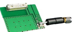
When specifying antennas for cellular or Industrial-Scientific-Medical (ISM) band applications below 900 MHz, the printed-circuit-board (PCB) size will greatly affect the average gain and efficiency of an installed antenna. Flex antennas and their feed lines (often with miniature U.FL RF connectors) typical employ radiation from the feed line as part of the antenna’s total radiation pattern.
Because of this, feed line routing will have a huge impact on the performance and antenna patterns produced by a flex antenna on a particular PCB design. Lacking actual antenna pattern data for such an installation, the data sheet gain presented for an omnidirectional antenna is likely to be peak gain (measured in some random direction).
System integrators often explain that they buy “premium” antennas for their system design rather than low-cost antennas with inferior performance. Suppliers of low-cost components such as antennas may take shortcuts in terms of production-line testing to reduce their operating cost, and the impact can often be seen in the poor quality of the final product.
Still, the old adage that “price equals quality” may not always ring true, or always guarantee higher performance simply because on antenna costs more than another. One way to verify whether a higher price has resulted in higher performance is by antenna performance testing in a qualified test laboratory. The investment in testing verifies critical antenna performance parameters and eliminates any questions about the antenna’s contributions to system-level performance.
Some system integrators forego antenna testing because their designer or contractor has performed extensive computer simulations on the antenna and these simulations show the antenna’s performance to be a close match to the system’s requirements. Simulations are a wonderful tool in hardware development and optimization, but they have never taken the place of hardware or system verification. No circuit designer would skip their hardware testing based on simulations.
Any antenna designer worth their salt will want verification, as well. Antenna testing is inexpensive compared to total product development costs, and antenna testing can reveal any performance nuances that might have been missed by the software in a computer simulation. In addition, the antenna test data from a qualified test laboratory can be incorporated into further computer simulations to improve the efficiency and effectiveness of antenna performance optimization.
Product developers have noted that their chip antenna has been tested by the antenna’s manufacturer, and they are now following the antenna supplier’s recommendations for installation on a PCB. Unfortunately, every PCB design is different and achieving optimal performance is never simply a matter of using a “cookbook” PCB layout.
Antenna component manufacturers provide a great deal of layout guidance and minimum circuit-board sizes to guide the best use of their products. To produce the performance levels shown on antenna data sheets, antenna suppliers typically perform testing of an antenna as part of an optimized demonstration board, with additional layouts developed as iterations of that demonstration circuit board.
But in an actual application, the clutter presented by surrounding structures—such as batteries, cables, and displays—can adversely affect the performance of a PCB-mounted antenna in ways that testing and even simulations cannot reveal. To save time and anguish as part of the design process, an antenna testing service can characterize an antenna embedded on a blank PCB representing the potential final design, with or without additional components mounted to learn more about how the antenna’s performance will appear in the final design.
Product developers have at times assumed their antennas are good enough without testing since prototype designs are providing suitable levels of overall performance during data-link testing under laboratory conditions. But such casual communications link tests with prototypes often do not yield enough information about the antennas or the full product design under all operating conditions.
Full design verification requires more extensive testing, such as waveform analysis on an oscilloscope or signal analyzer. Qualified antenna test laboratories can provide more extensive test data on active or passive antennas to help better understand results from link testing.
Often, a particular antenna may be deemed acceptable for a new design because it has been used successfully in the past. But this assumption may also be part of the perpetuation of mediocre performance in a new product. The thinking that “this is the way it’s always been done” will not lead to reaching new performance levels. Verifying the performance of an antenna should be considered as part of adding an improvement to a new product design. A properly verified antenna design can then be reused with confidence.
When the PCB for a new product design passes FCC/EN radio compliance testing, the antenna is often assumed to be acceptable, with no need of further testing. But compliance testing focuses on controlling interference that could be originating from a new radio design. Various spurious emissions and band edge checks are made in detail, along with a few other modulation parameters, but such testing does not attempt to quantify the antenna performance.
For example, such testing will not reveal whether an antenna is inefficient or exhibits unintentional directivity. More extensive testing can reveal such behavior and lead to the use of a different antenna and an improvement in the new product design.
Antenna performance is often assumed to be good when an antenna shows good VSWR or return loss during testing with a vector network analyzer (VNA). But antennas with return loss of better than 10 dB have also been found to suffer from poor radiation efficiency (less than 10%). When a chip antenna layout (or an all-copper PCB antenna) has a particularly poor return loss, a great deal of trial-and-error impedance matching can result in the addition of inductive/capacitive (L/C) impedance-matching components that seem to help.
However, with VSWRs above 10:1 or more, there can be a large amplification of current in impedance-matching inductors and boost of voltage in impedance-matching capacitors, multiplying their inherent losses. The high losses of these components masquerade as radiation resistance, even though the antenna may not be practically matchable. This is a case where the matching components yield a “good match” by absorbing RF energy, not by transferring it to a radiating antenna.
One way to learn if this may be happening to a circuit design is to perform the “hand test,” by waving a hand over a board and its antenna and monitoring the effects on return loss measurements. If there are no effects from the hand being in close proximity to the circuit board and its antenna, then the design is acting as a dummy load rather than an antenna. In addition, if a compact antenna exhibits unexpectedly wide return-loss bandwidth, it is probably a result of high internal losses and not the radiation resistance.
System designers fail to test an antenna for a new design because it works well in free space. But for the same reasons noted earlier, an embedded antenna will be affected by surrounding hardware, such as cables, shields, displays, and other components mounted on a PCB or within a product enclosure. Any structures that are within a quarter wavelength of the antenna must be considered part of the antenna.
Those structures will absorb RF energy and lower the antenna’s efficiency while also reflecting energy and causing unexpected changes to an antenna’s radiation pattern. Fortunately, antenna pattern measurements at a qualified test facility can provide the data needed for optimum antenna placement.
The simple assumption that an antenna manufacturer meets its published specifications has been a long-running excuse not to perform additional antenna measurements. But failure to meet those specifications will impact the performance of a new product design using that antenna, making it worthwhile to perform additional antenna characterization at a qualified test facility. When those measurements reveal differences from the published data sheets, these results should be shared with the supplier of that antenna.
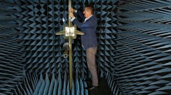
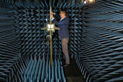
An antenna test laboratory can fortify a design with an independent evaluation of its antenna, performed in an anechoic chamber. As mentioned earlier, testing is relatively low in cost, with complete radiation pattern testing performed over wide swept-frequency ranges from facilities such as Antenna Test Lab Co. for as little as $450. Data can be provides for a large number of parameters, including gain; radiation efficiency; VSWR (return loss); radiation patterns in boresight, polar, or spherical formats (1D, 2D, or 3D formats); left-hand-circular-polarization (LHCP) gain; right-hand circular polarization (RHCP) gain; and axial ratio. The test results can provide insights into antenna performance that leave nothing to chance as part of a larger design.
Glenn Robb is the founder and principal engineer of Antenna Test Lab Co.


