This file type includes high resolution graphics and schematics.
Amplification at 2.4 GHz is necessary for a number of different wireless applications, and CMOS offers a low-cost and effective process for achieving respectable gain at that frequency. In support of wireless transmitters at 2.4 GHz, a 2.4-GHz CMOS current-mode power amplifier was developed for improved efficiency. It consists of two differential amplifier stages. The first stage is a driver evolved from current mirrors, while the second stage is a current-mode Class D amplifier. All components, including the inductors, are on the CMOS chip. Simulations performed with a commercial computer-aided-engineering (CAE) software package (from Cadence Design Systems) indicate high power-added efficiency (PAE) of 40% with 0.25-W saturated output power and high gain when operating at a 3.3-VDC supply.
The rapid growth of wireless devices and services has driven the need for practical solid-state devices, including amplifiers. Many applications are being served by single-chip radios.1 Many of the RF front-end functions, such as the low-noise amplifier (LNA), frequency mixer, and voltage-controlled oscillator (VCO) serving as the radio’s local oscillator (LO) have been integrated onto a single chip using silicon CMOS processes. But some of the limitations of CMOS technology—such as thermal dissipation, power efficiency, and supply voltage—have prevented the integration of the power amplifier (PA) output stage.2
Related Articles
• Integrated BiCMOS Chip Set Covers 400 GHz
• CMOS LNA Serves Flat Gain To 5 GHz
• CMOS Switches Extend Control To 8 GHz
Of course, the PA is a key part of a 2.4-GHz wireless radio, supporting the transmitter section. PA performance can be judged by a number of parameters, including output power, gain, and efficiency, with one of the more important characteristics (especially for extended battery life) being the efficiency.3 High efficiency can also translate into less heat produced by the output circuitry.
A number of different topologies have been applied for RF PAs, differentiated by the operational states of the active devices (transistors). For example, different classes of linear PAs—including Classes A, B, and C—refer to the use of a constant power supply in energizing the transistors. In contrast, switched-mode PAs— such as Classes D, E, and F—turn the power supplies on and off.4 Each of these types of PA have advantages and disadvantages: Linear amplifiers offer good linearity at the expense of efficiency, while switched-mode amplifiers sacrifice linearity for efficiency.
Class D switched-mode amplifiers have often been used for low-frequency applications, but less so at higher frequencies. At the latter frequencies, the parasitic capacitance discharge losses become excessive. But a modified Class D structure, known as a current-mode Class D (CMCD) PA uses zero voltage switching (ZVS) to minimize discharge losses and can work at higher frequencies.5-8 Most current-mode Class D PAs have been fabricated with gallium arsenide (GaAs) field-effect transistors (FETs)5,6 or silicon lateral diffused metal-oxide-semiconductor (LDMO) FETs.7,8 The use of these technologies prevents fabrication as a silicon CMOS chip.
A two-stage amplifier was designed for high efficiency in a silicon CMOS process. The first, driver stage accepts input current signals and converts them to larger driving signals for the following stage. The second stage is basically a PA. Spiral inductors were used to allow the use of on-chip inductors. For analysis, the amplifier design was simulated using the Cadence Spectre® CAE program for a CHRT 0.18-μm mixed-signal/RF CMOS process. The simulations revealed that this PA design offers higher efficiency and output power than other CMOS PAs working at the same frequency.9-13
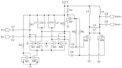
Figure 1 presents the circuit for this high-efficiency CMOS PA. The driver stage, which derives from current mirrors, consists of resistors R1, R2, and R3; capacitors C1, C2, C3, and C4; inductors L1 and L2; and transistors M1 through M6. The output stage consists of capacitors C7, C8, and C9; inductors L3, L4, and L5; and transistors M8 and M9. It is based on a CMCD structure to provide high efficiency at high frequencies. Capacitors C5 and C6 are blocking capacitors, while resistors R4 through R6 and transistor M7 constitute the bias circuitry for the switching transistors. The PA accepts a current input signal and delivers a voltage output, in effect operating as a transimpedance amplifier (TIA).
1. This schematic diagram shows the circuit elements and layout for the high-efficiency, 2.4-GHz silicon CMOS power amplifier.
The PA’s driver stage consists of three current mirrors. The amplification principlefor this stage is based on the proportional relationship of the current mirror. If the two transistors of the current mirror operate in their saturation region, and their drain currents are proportional according to the widths of the transistors, the principle can be described by Eq. 1:
iM2 = (W2/W1) iM1 (1)
where:
iMk = the drain current of transistor Mk and
Wk = the width of transistor Mk.
The drain current consists of a DC component and an AC component. The input and output signals are the AC components. The relationship of the input and output signals can be described by Eq. 2:
vOUT = (W2/W1) iin(ZP) (2)
where:
vout = the output voltage signal;
Zp = the impedance of the shunt-resonant circuit C3L1 at the working frequency; and
iin = the input current signal.
When the proportionality factor is larger than unity, the current mirror can be used as an amplifier.The two current mirrors, M1-M2 and M3-M4, are used to amplify two differential input signals separately. Current mirror M5-M6 can control the direct current of the driver stage. The following analysis will show how this works.
From the schematic diagram of the PA in Fig. 1, Eq. 3 can be easily obtained:
im6 = im1 + im2 + im3 + im4 + Im1 + Im2 + Im3 + Im4 (3)
where:
iMk = the drain current of transistor Mk;
iMk = the AC component of iMk; and
IMk = the DC component of iMk.
It is known that the input signal is a differential signal with 180-deg. phase difference. The relationship can be tracked by means of Eq. 4:
im1 = -im4, im2 = -im3 (4)
Substituting Eq. 4 into Eq. 3 yields Eq. 5:
iM6 = IM1 + IM2 + IM3 + IM4 (5)
Since iM6 = (WM6/W5)iM5, Eq. 6 can be found:
IM1 + IM2 + IM3 + IM4 = (W6/W5)iM5 (6)
The left-hand side of Eq. 6 shows the direct current of the PA’s driver stage. On the right side, current iM5 is tied to resistor R3. The direct current of the driver stage can be controlled by adjusting the width of transistors M5 and M6 and the resistance of R3. From this analysis, it can be seen that the driver stage has three functions. First, it can accept the input current wave signal, this is in accordance withthe demand of current mode circuit. Second, it has high gain and provides enough driving voltage for the following stage. Third, the structure of the driver stage can control the power dissipation, and it is helpful for increasing the efficiency of the PA.
This file type includes high resolution graphics and schematics.
A critical part of the PA circuit design is the output stage, which adopts a CMCD structure. It consists of transistors M8 and M9, LC tank capacitor C7, inductor L5, and two large inductors L3 and L4 (Fig. 1). For good output impedance matching, inductors L3 and L4 are adjusted to 3.23 nH. The resonator formed by capacitor C7 and inductor L5 resonates at the working frequency (2.4 GHz).
Driven by differential input signals (with 180-deg. phase difference), transistors M8 and M9 alternately turn on and off. The large inductors L7 and L8 work as RF chokes. They are meant to provide the constant direct current Idc. When transistor M8 turns on and transistor M9 turns off, direct current Idc channels through the LC tank from the right side to the left side. When transistor M9 turns on and transistor M8 turns off, the reverse happens. This results in a square-wave current at the LC tank. According to the Fourier transform of a square wave, the square-wave current includes a great deal of harmonic content.
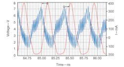
Fortunately, due to the symmetry of the PA’s circuit and the selectivity of the parallel LC tank, all high-order harmonics are minimized. Only the fundamental current component can cause a sinusoidal voltage wave at the parallel LC tank. The loads connected to the LC tank receive a complete sinusoidal voltage. Figures 2 and 3 show ideal voltage and current waveforms, respectively, for switching transistors M8 and M9.
2. This plot provides the drain-source voltage characteristics of switching transistor M8.
3. This plot shows the drain current characteristics of switching transistor M8.
As Figs. 2 and 3 indicate, the drain-source voltage of switching transistor M8 is a half sinusoidal wave. The corresponding current through switching transistor M8 is a square wave with amplitude of 2Idc and duty cycle of 50%. Alternately, the transistor exhibit zero values of current and voltage. In this circuit, the output power is equal to the voltage multiplied by the current. Although in theory a CMCD PA can achieve high efficiency, it is limited in its frequency of operating. This is because parasitic-based losses increase rapidly as frequency increases. Energy loss per cycle, Ec, can be found by means of Eq. 76:
Ec = 0.5Cv2 (7)
where:
Ec = the energy loss;
C = the drain-source parasitic capacitance; and
v = the drain-source voltage when the transistor is turned on.
The CMCD PA has a ZVS characteristic, which means that the drain-source voltage is zero when the transistor is turned on. According to Eq. 7, charge losses can be avoided, so that the CMCD PA can work well at higher (RF) frequencies.
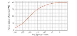
4. This plot offers the power-added efficiency (PAE) of the 2.4-GHz CMOS amplifier.
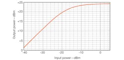
5. The CMOS PA’s output power is plotted here as a function of input power.
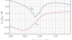
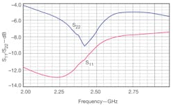
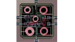
Figure 4 plots the power added efficiency (PAE) of the PA when the input power is varied. The PAE begins to drop when the input power falls to 0 dBm. The maximum PAE is about 40%. Figure 5 shows variations in output power. The maximum output power of +24 dBm is achieved with an input power level of 0 dBm. The PA’s gain is about 24 dB. Figure 6 shows the amplifiers input/output matching, with S11 exceeding -11 dB and S22 exceeding -8.8 dB. Figure 7 shows the drain current and voltage for transistor M8. As can be seen, the current wave is a square wave, while the voltage is a half-period sinusoidal wave. Figure 8 shows the PA’s chip layout, with a die size of 0.82 x 0.80 mm.
6. The CMOS PA’s S11 and S22 characteristics are shown here.
7. These plots show the drain current and voltage for switching transistor M8.
8. The CMOS PA was fabricated with on-chip passive circuit elements as a single chip, with the layout shown here.
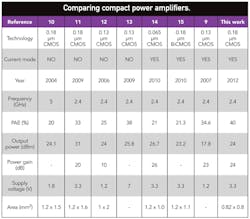
The 2.4-GHz CMOS power amplifier compares well with amplifiers developed in previous studies (see table). It achieves the gain of earlier 2.4-GHz amplifier designs, but with considerably higher efficiency. The new current-mode amplifier, with its reasonable output power and high efficiency, is suitable for a number of mobile wireless communications applications at 2.4 GHz.
College of Information Science and Engineering, Hunan University, Changsa, 410082, People’s Republic of China, e-mail: [email protected]
C.W. Chan, ProfessorEnergy Informatics Laboratory, Faculty of Engineering and Applied Science, University of Regina, Regina, SaskatchewanS4S 0A2, Canada
Hongxia Yin, Lecturer
Wenbin Huang, Graduate Student
College of Information Science and Engineering, Hunan University, Changsa, 410082, People’s Republic of China.
Acknowledgments
This work was supported in part by the Open Fund Project of Key Laboratory (No. 12K012) and Young Teachers Program in Hunan Universities. The authors would like to thank the anonymous reviewers for their valuable suggestions, which helped improve the quality of the paper.
References
1. Riccardo Brama and Luca Larcher, “A 30.5 dBm 48% PAE CMOS Class-E PA with Integrated Balun for RF Applications,” IEEE Journal of Solid-State Circuits, Vol. 43, No. 8, August 2008.
2. Ayman O. Ameen and Khaled M.Sharaf, “A 1.75 GHz CMOS Class E RF Power Amplifier and Oscillator,” IEEE International Conference on Microelectronics, 2007.
3. Boshi Jin and Qun Wu, “Fully Integrated CMOS Power Amplifier Design for WiMAX Application with Semi-lumped Transformer,” IEEE International Conference on Industrial Informatics, Daejeon, Korea, July 2008.
4. Sherif A. Mohamed and Yiannos Manoli, “A Differential Common-Gate Class-E Power Amplifier with Positive-Negative Feedback,” IEEE International Midwest Symposium on Circuits and Systems, 2009.
5. H. Kobayashi, J.M. Hinrichs, and P.M. Asbeck, “Current Mode Class-D power Amplifiers for High Efficiency RF Applications,” IEEE. Transactions on Microwave Theory & Techniques, Vol. 49, No. 12, December 2001.
6. Tsai-Pi Hung and Andre G. Metzger, “Design of High-Efficiency Current-Mode Class-D Amplifiers for Wireless Handsets,” IEEE Transactions on Microwave Theory & Techniques, Vol. 53, No. 1, January 2005.
7. Ji-Yeon Kim and Dong-Hoon Han, “A 50 W LDMOS Current Mode 1800 MHz Class-D Power Amplifier,” IEEE International Microwave Symposium Digest, 2005.
8. Christian Schuberth and Peter Singerl, “Design of a Current Mode Class-D RF Amplifier Using Load Pull Techniques,” IEEE International Microwave Symposium Digest, 2009.
9. Chungyu Wu, Shunwei Hsu, and Wenchieh Wang, “A 2.4-GHz CMOS Current-Mode Power Amplifier with High PAE and Output Power,” IEEE International Symposium on Circuits and Systems, 2007.
10. YunSeong Eo and KwangDu Lee, “A Fully Integrated 24-dBm CMOS Power Amplifier for 802.11aW LAN Applications,” IEEE Microwave & Wireless Components Letters, Vol. 14, No. 11, November 2004.
11. Kyu Hwan An and Dong Ho Lee, “A 2.4-GHz Fully Integrated Linear CMOS Power Amplifier with Discrete Power Control,” IEEE Microwave & Wireless Components Letters, Vol. 19, No. 7, July 2009.
12. Gang Liu, Tsu-Jae King Liu, and Ali M. Niknejad, “A 1.2-V, 2.4-GHz Fully Integrated Linear CMOS Power Amplifier with Efficiency Enhancement,”IEEE Custom Integrated Circuits Conference, 2006.
13. Hafez Fouad, Abdel-halim Zekry, and Khalid Fawzy, “Self-Biased 0.13-μm CMOS 2.4-GHz Class E Cascode Power Amplifier,”26th National Radio Science Conference, New Cairo, Egypt, March 2009.
14. Mingyuan Li, Ali Afsahi, and Arya Behzad, “A Single-Chip 2.4-GHz Double Cascode Power Amplifier with Switched Programmable Feedback Biasing under Multiple Supply Voltages in 65-nm CMOS for WLAN Application,” IEEE Journal of Radio Frequency Integrated Circuits Symposium, 2010.
15. Ying Ruan, Lei Chen, Yan-hua Liu, Feng Ran, and Zong-sheng Lai, “A 2.4-GHz Monolithic SiGe Power Amplifier for Wireless-LAN Transceiver,” Microelectronics and Electronics (Prime Asia), 2010 AsiaPacific Conference on Postgraduate Research.
This file type includes high resolution graphics and schematics.
