Pointing to Progress in Probe Stations
Download this article as a .PDF
Wafer probes and probe stations are marvels of mechanical engineering. They are capable of delicately maneuvering measurement probe contacts onto micron-sized circuit features with enough contact force to make meaningful measurements without causing damage to the circuits. As semiconductor wafers have grown in size, designers of wafer probe stations have responded with probe stations capable of handling larger wafers with precision. At higher frequencies, it is the precision needed for millimeter-wave S-parameter measurements. Modern probes and probe stations provide the placement precision for on-wafer measurements to 70 GHz and beyond.
Semiconductor wafer probing systems are available as manual, semi-automated, and fully automated systems. Working with test probes mounted in micro positioners, they can achieve the precision needed to place a probe tip onto a miniature test point, such as an IC’s probe pads. With that contact made, microwave test equipment such as a vector network analyzer (VNA) can be used to characterize circuit or device electrical behavior for modeling and packaging purposes.
As ICs move towards higher frequencies and smaller wavelengths, device dimensions continue to shrink, requiring even greater probe placement precision. Semiconductors are typically designed with probe contact pads as part of the circuit, but getting to these pads with the tip of an electrical probe requires positioning precision in all three axes. This is accomplished by a combination of probe station components, including the main probe station to hold and position a circuit under test and micro positioners to hold and position test probes.
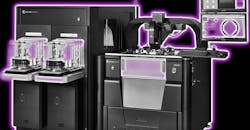
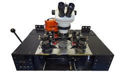
In the case of the CM300xi probe station (Fig. 1) from Cascade Microtech, computer intelligence guides the probe positioning accuracy. Using what the company calls “Contact Intelligence” technology, this probe station detects on-chip probe positions and includes the effects of operating temperature when controlling the placement of the probe tip. In this way, the automated probe station can achieve the most-accurate probe-to-pad alignment possible for a measurement, covering a wide range of semiconductor materials, wafer sizes, and devices.
The CM300xi probe station is modular and scalable, allowing a user to equip the system with as much or as little capability as needed. The system can handle 200- and 300-mm wafers, with an x-y travel range of 301 × 501 mm (11.9 × 19.7 in.). Movement is controlled by micro stepper motors with moving stages traveling on precision ball bearings. Placement accuracy in the x and y directions is better than 2 μm in standard operating mode and better than 0.3 μm in precision mode, with positioning speed of 50 mm/s (2 in./s). The z-axis stage moves with just as much precision over a travel distance of 10.0 mm (0.39 in.) The positioning accuracy in the z-axis is better than 2 μm, with repeatability of better than 1 μm. The positioning resolution in all three axes is 0.2 μm.
In addition to the Contact Intelligence capabilities, the CM300xi probe station is guided by the company’s VueTrack software for rapid and accurate alignment of probe tips to probe pads. In addition, the Velox probe station control software simplifies the programmable operation of the probe station and integration with test equipment for fast, reliable automated measurements without causing damage to wafers under test (or probe tips, for that matter). For those who prefer, an open, non-EMI-shielded version of the system is also available without the Contact Intelligence technology. The company also produces systems for performing wafer-level-reliability (WLR) testing. The Estrada system, for example, can perform high-volume reliability testing on 300-mm wafers.
Exploring Other Options
While Cascade Microtech may have done as much as any one company to define the current state of RF/microwave wafer probe technology, probe stations suited for RF/microwave probing are available from a number of other suppliers, including D-Coax, Lake Shore Cryotronics, MicroXact, and SIGNATONE.
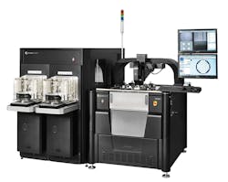
For example, D-Coax offers its D14 probe station (Fig. 2) for those on tight budgets. It is a versatile manual system with independent vacuum control to accommodate micro positioners for wafer diameters of 3, 6, 8, 10, 12, and 14 in. It incorporates 17 independently operated vacuum positions for calibration substrates and other devices and includes vibration-isolating feet in a relatively small footprint. In support of the probe station, the company provides RF/microwave probes, coaxial cable assemblies to 67 GHz for interconnections to test equipment such as VNAs and calibration substrates. It also recommends RF/microwave probes from GGB Industries.
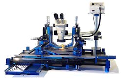
In some cases, such as for R&D, automation may not be needed and a manual probe station may provide the capability required to probe a packaged or unpackaged device. The WL-210 RF/microwave probe station (Fig. 3) from SIGNATONE is a member of the company’s WAVELINK family of RF/microwave wafer probe stations. The WL-210, which can handle wafers as large as 8 in., features a base formed of 2-in.-thick aircraft-grade aluminum for stability. The probe station is designed not to resonate and weighs about 200 lb. (91 kg).
It has three substrate sites for mounting various formats of calibration substrates and is capable of probing wafers, packaged devices, and even printed-circuit boards (PCBs). The x-y stage has a full travel range of 200 × 200 mm by means of carriage-and-rails bearings and a rotary control. The resolution of the x-y stage movement can be set coarse (5 mm/turn) or fine (0.5 mm/turn). It features a nonferrous chuck and stage and supports a variety of micro positioners, including with magnetic base, vacuum, and bolt-down configurations.
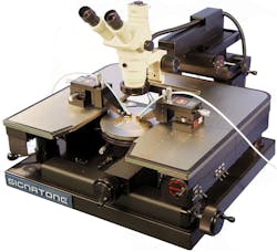
Similarly, the SPS-2000 probe station (Fig. 4) from MicroXact is a fully manual station with x-y range of travel of 100 × 100 μm or more and 5 μm positioning resolution. Standard SPS-2000 probe stations are designed to handle wafers with diameters as large as 100 μm, although stations with larger capacities can be provided. Numerous options are available, including a vibration isolation table, three-axis micro positioners, and precision microscopes.
For RF/microwave probe-based measurements, precision is needed—not just to prevent damage to the circuit under test, but also to preserve a typically expensive test probe. Tight control over the z-axis motion can help prevent probe tip damage and provide repeatable electrical contacts for testing.
Although measurements with a test probe are normally associated with on-wafer circuits, the increasing use of millimeter-wave frequencies for automotive radar systems and 5G wireless networks will prompt the use of “wafer” probes for an increasing number of non-wafer circuits, including PCB modules for millimeter-wave applications. The speed and accuracy of RF/microwave probe stations will contribute a great deal to enabling the commercialization of millimeter-wave circuits.

About the Author
Jack Browne
Technical Contributor
Jack Browne, Technical Contributor, has worked in technical publishing for over 30 years. He managed the content and production of three technical journals while at the American Institute of Physics, including Medical Physics and the Journal of Vacuum Science & Technology. He has been a Publisher and Editor for Penton Media, started the firm’s Wireless Symposium & Exhibition trade show in 1993, and currently serves as Technical Contributor for that company's Microwaves & RF magazine. Browne, who holds a BS in Mathematics from City College of New York and BA degrees in English and Philosophy from Fordham University, is a member of the IEEE.
