This file type includes high resolution graphics and schematics when applicable.
Traditional spectrum analyzer measurements of RF device performance are classically measurements of non-linear performance such as harmonics, Third-Order Intercept (TOI) or input-related spurious responses. A very common non-linear measurement that is made is the adjacent channel power measurement that determines the amount of power relative to the power in the channel that appears in adjacent channels. These types of measurements tend to predict how spectrally pure a given RF device will perform when multiple receivers or transmitters are present.
Modern signal analyzers retain the ability to make these classic non-linear distortion type measurements as well as in-channel phase and flatness distortion-type measurements. These types of impairments are linear distortion. An example of this is a power amplifier that may have exceptional non-linear performance. The performance could be a very high TOI capability with extremely low harmonics distortion. However, the amplitude flatness across the band of interest might be enough to effect on the radiated signal. This may have no effect on a narrow bandwidth analog modulated signal, but variance in amplitude versus frequency can have a significant impact on the quality of a wide-bandwidth digitally modulated signal. Emerging modulation formats are in general getting wider in bandwidth, where the phase and frequency performance of the RF device and components requires increasingly more stringent methods for measuring this performance.
Frequency Distortion
A simple example of frequency distortion can be applying an amplitude-modulated signal with 100% depth of modulation, where the modulating signal is a 1-MHz sine wave, to the input of an amplifier. We expect a carrier with two sidebands, 1 MHz above and below the carrier. In a perfect system, the two sidebands will be equal in amplitude and 6 dB below the amplitude of the carrier. During a single cycle, the sidebands will constructively add in voltage to double the amplitude of the resultant signal and destructively combine to reduce the resultant signal to zero volts. This is true only if the two sidebands are not affected by changes in their phase and amplitude due to amplitude flatness or phase linearity issues in the passband of the amplifier. These can result in the sidebands amplitude no longer being equal, or the phase relationship is no longer maintained due to time delays within the passband of the amplifier. A non-uniform phase or frequency response will cause distortion to the signal that was not present in the original signal.
One method for measuring these effects is to input to the amplifier multiple carriers evenly spaced across the bandwidth of interest, and measuring both the resultant amplitude and phase of each of the carriers. This is more of a mental exercise for small systems, but this technique also works well for more complex systems that employ multiple downconversion stages and digitizers where the complete system can be tested.
In practice, measurements such as error vector magnitude (EVM), code domain power and spectral flatness are in-channel measurements that provide insight into the performance of a particular communication system. These measurements, when used in combination with non-linear measurements such as adjacent channel power (ACP) and harmonics, provide for a complete understanding of the performance of the physical layer of a communication system.
Error Vector Magnitude (EVM)
The EVM measurement has become an invaluable tool for most technicians and engineers because it can verify the performance of a complex modulated communication device as well as troubleshoot a communication issue to root cause. A signal analyzer is most commonly used for this type of measurement and, in most cases, the user simply sets up the signal analyzer by providing the modulation type, symbol rate and filter type used in the creation of the signal. The signal analyzer then demodulates the signal and creates an ideal mathematical representation of the signal in its in-phase and quadrature components, and then compares it to the actual measured signal. EVM is the root mean square (RMS) of the error vectors, computed and expressed as a percentage of the square root of the mean power of the ideal signal. The error vector is the magnitude of the vector at the detected symbol location (refer to the EVM phasor diagram in Fig. 1).
Mathematically it can be expressed as:
Where:
[n] = measurement at the symbol time
Ierr = Iref - Imeas
Qerr = Qref - Qmeas
The image in Fig. 2 is the constellation diagram of a quadrature phase shift keying (QPSK) signal where the Y-axis is the quadrature component and the X-axis is the in-phase component. The red dots in the four quadrants represent the In-phase and quadrature values at each of the symbol times.
A gain imbalance in the system will be observed as non-equal amplitudes in either the in-phase or quadrature axis. A circular rotation of the symbol points is normally an indication that a spurious signal is present below the envelope of the modulated signal. Excessive phase noise will result in a skewing of the symbol points. Spreading of the symbol points is normally an indication of either phase linearity or amplitude flatness issues.
The overall EVM results are shown in Fig. 3.
The RMS EVM result is displayed as well as the magnitude and phase components to assist troubleshooting if needed. Sources in error are most commonly found in IF phase linearity, amplitude flatness, or contributions from the phase noise in the system. Gain imbalance can easily be measured and adjustments made if needed.
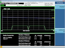
In some systems it is possible to measure the spectral flatness directly. This can be done with an orthogonal frequency-division multiplexing (OFDM) signal that inherently has multiple carriers across the bandwidth of interest. These systems may have bandwidth requirements as high as 2 GHz. Maintaining a flat frequency response across this large frequency interval is very difficult, and normally the receiver will need to apply equalization to compensate for the non-flat frequency response. Figure 4 shows an example of a spectral flatness measurement on a 802.11n WLAN signal.
The spectral flatness measurement allows the user to observe the amplitude flatness of the entire system at a glance. In this case, the spectral flatness is well within specification with sufficient margin. In cases where there is limited bandwidth, you will observe roll-off in the upper and lower frequency edges or amplitude ripple within the band edges.
Summary
As communication systems become increasingly more complex, measurement techniques will continue to evolve to more quickly understand and quantify distortion that may be present in the system. These systems will need to be spectrally friendly in terms of making non-linear distortion type measurements, but also ensure that the spectrum used is done so efficiently. Reducing the error rates of signals will enable, in the end, more data for the same amount of spectrum.
This file type includes high resolution graphics and schematics when applicable.
