Network analyzers are indispensable test instruments in the RF/microwave industry. Their measurement capabilities allow them to characterize a wide range of devices, components, and systems. Many components—both passive and active—are commonly measured with a network analyzer, including amplifiers, filters, attenuators, switches, and many others.
Network analyzers are relied upon heavily for manufacturing production testing. A component’s datasheet typically contains a significant amount of information obtained from a network analyzer. In addition, network analyzers are used for research and development purposes. They can be used to measure engineering prototypes, thus allowing engineers to optimize performance characteristics like gain flatness and return loss.
What Network Analyzers Do
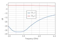
Network analyzers can measure and display a device under test’s (DUT) magnitude and phase information across a frequency range. A generic illustration of a network analyzer plot is shown in Figure 1. In essence, a network analyzer characterizes a DUT in terms of scattering parameters, or S-parameters.
1. This plot is a depiction of a network analyzer measurement.
S-parameters are used to characterize performance at RF and microwave frequencies in terms of incident and reflected waves. S-parameters are vector quantities, meaning they contain both magnitude and phase information. A scalar network analyzer (SNA) can only measure magnitude, while a vector network analyzer (VNA) can measure both magnitude and phase. Each of these will be discussed in more detail later.
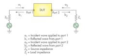
Figure 2 shows an illustration of a two-port network. 50-Ω impedances are typical of most RF/microwave applications. Hence, ZS and ZL in Fig. 2 would generally be 50 Ω. Cable-television (CATV) applications are the main exception, as they operate in a 75-Ω environment.
2. Shown is a two-port network.
Figure 3 is based on the network shown in Fig. 2. Here, ZS and ZL are equal to 50 Ω. Port 2 of the DUT is terminated in a 50-Ω load, thus setting a2 to be equal to zero.
3. In this figure, an incident wave, a1, is applied to the DUT.
In Fig. 3, a1 is applied to Port 1 of the DUT. A portion of this incident wave is transmitted through the DUT and exits through Port 2, thereby resulting in b2. A portion of the incident wave is also reflected back to the source, thereby resulting in b1. Now, two S-parameters, S11 and S21, can be mathematically defined as follows:
Figure 4 is also based on the network shown in Fig. 2. Here, Port 1 of the DUT is terminated in a 50-Ω load, thus setting a1 to be equal to zero.
4. Here, an incident wave, a2, is applied to the DUT.
In Fig. 4, a2 is now applied to Port 2 of the DUT. A portion of this incident wave is transmitted through the DUT and exits through Port 1, thereby resulting in b1. A portion of the incident wave is also reflected, thereby resulting in b2. Now, the two remaining S-parameters, S12 and S22, can be mathematically defined as follows:
A two-port network therefore has four S-parameter elements: S11, S21, S12, and S22. S11 and S22 are known as reflection coefficients. S21 and S12 are known as transmission coefficients. Furthermore, a network can be defined in matrix form, known as an S-parameter matrix. The S-parameter matrix of the two-port network discussed previously is shown as:
As stated earlier, S-parameters contain both magnitude and phase information. Magnitude is typically expressed in decibels (dB). This is mathematically defined as:
The dB representations of S11 and S22 are known as return loss, which is the difference in dB between the reflected signal and the incident signal. Thus, a return loss of −15 dB means that the reflected signal is 15 dB lower in magnitude than the incident signal. Return loss is commonly expressed as a positive value, so a return loss of −15 dB is often expressed as just simply 15 dB.
The magnitude element of S21 is known as gain or insertion loss, depending on whether the DUT is active or passive. In other words, an active device—such as an amplifier—has gain because it increases the magnitude of an input signal. A passive component like a filter does not have gain, meaning the output signal is smaller in magnitude than the input signal. In this case, S21 is referred to as insertion loss. S12 defines transmission in the reverse direction. Thus, it’s known as reverse gain or reverse transmission.
It’s often important to characterize phase along with magnitude. As discussed already, when an incident signal is applied to a DUT, a portion of that signal is transmitted. The transmitted signal that exits the DUT differs not only in magnitude from the incident signal, but also in phase. Hence, S21 and S12 also describe the phase difference in degrees between a transmitted signal and an incident signal. A linear phase response over frequency is desirable—deviating from one can cause distortion.
Group delay is the transit time of a signal as it passes through a DUT. It’s mathematically defined as the negative of the derivative of phase response with respect to frequency, meaning that it quantifies phase linearity. Thus, a flat group delay means the phase response is linear. Network analyzers are commonly used to measure the group delay of components, such as filters.
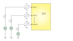
5. This figure shows a network with N ports.
The two-port model that has been discussed represents a component with two ports. However, many components have more than just two ports. Figure 5 shows an illustration of an N-port network. The DUT here could possibly be a power divider or some other component with multiple ports. The S-parameter matrix of this network is:
How Network Analyzers Work
The fundamental purpose of a network analyzer is to measure S-parameters. A network analyzer can be classified as either a VNA or an SNA. VNAs have become more widely used in recent years. However, let’s first discuss SNAs.
SNAs can only measure magnitude. They do not have the capability to perform phase measurements. SNAs perform transmission measurements by means of a diode detector, which converts an RF signal to a dc voltage. This dc voltage is proportional to the magnitude of the RF signal. Unfortunately, this process does not take phase information into account. Return loss measurements can be achieved by means of a directional bridge.
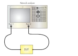
VNAs are much more powerful than SNAs, as they can measure both magnitude and phase. Figure 6 is an illustration of a VNA being used to measure a two-port component, such as a filter or amplifier. The input of the DUT is connected to the end of a cable that’s attached to Port 1 of the VNA. The DUT’s output is connected to the end of a cable that is attached to Port 2 of the VNA. The DUT shown in Fig. 6 essentially represents the DUT shown in Fig. 2.
6. Shown is a vector network analyzer (VNA) measuring a two-port component.
In Fig. 6, the VNA contains an RF source, which generates signals over the frequency range of interest. These signals exit through Port 1 and are applied to the DUT. When a signal at any frequency is applied to the DUT, a portion of that signal is transmitted through the DUT to Port 2 of the VNA. Another portion is reflected back to Port 1. The user can then see S21 or S11 measurements on the VNA’s display.
To measure S22 or S12, the VNA generates signals that exits through Port 2 and are applied to the DUT. A portion of a signal at any frequency applied to the DUT now transmits through the DUT to Port 1 of the VNA. Another portion is reflected back to Port 2. Now, the user can see S12 or S22 measurements on the display.
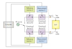
The VNA’s architecture can now be examined to understand how these measurements are achieved. Figure 7 shows a general block diagram of a VNA with two test ports. (It should be noted that Fig. 7 shows a general VNA architecture. Additional variations are possible, but the general concept remains.) The signals generated by the VNA’s RF source enter a switch, which routes the signal toward either Port 1 or Port 2.
7. Here’s a simplified block diagram of a VNA with two test ports.
To measure S11 or S21, the switch would route the signal toward Port 1. The signal first enters a directional device, shown as Directional Device R1 in Fig. 7. This directional device could be a directional coupler or bridge. A power divider could also be used here. The purpose of this device is to direct a portion of the input signal to a reference receiver, shown as Reference Receiver 1. Once the signal enters this reference receiver, it’s downconverted and ultimately processed.
The signal that passes through Directional Device R1 then passes through another directional device, shown as Directional Device M1 in Fig. 7, before arriving at the DUT. When the signal does arrive at the DUT, a portion is reflected back to Port 1 of the VNA and reenters Directional Device M1. This device now directs a portion of the reflected signal to a measurement receiver, shown as Measurement Receiver 1. Next, this signal is downconverted and processed. The VNA can then compare the data obtained from Measurement Receiver 1 with the data obtained from Reference Receiver 1. This process summarizes how S11 is measured.
The signal applied to the DUT also results in a transmitted signal, which exits the DUT and enters Port 2 of the VNA. This transmitted signal enters another directional device, shown as Directional Device M2 in Fig. 3-7. This device directs a portion of the signal to another measurement receiver, shown as Measurement Receiver 2. This signal is subsequently downconverted and processed. Now, the VNA can compare the data obtained from Measurement Receiver 2 with the data obtained from Reference Receiver 1. This process summarizes how S21 is measured.
To measure S22 or S12, the switch would route the signal to Port 2. The same process occurs in the opposite direction: The signal first enters Directional Device R2 in Fig. 7, which directs a portion of the signal to Reference Receiver 2. After entering this reference receiver, the signal is downconverted and processed.
The signal that passes through Directional Device R2 then passes through Directional Device M2 on its way toward the DUT. After arriving at the DUT, a portion of the signal is reflected back to Port 2 of the VNA and reenters Directional Device M2. Now, a portion of this reflected signal is directed to Measurement Receiver 2. Afterward, this signal is downconverted and processed. The data obtained from Measurement Receiver 2 can then be compared with the data obtained from Reference Receiver 2, thus summarizing the S22 measurement process.
The signal that’s transmitted through the DUT enters Port 1 of the VNA. This transmitted signal enters Directional Device M1 in Fig. 7, which directs a portion of the signal to Measurement Receiver 1. This signal is likewise downconverted and processed. The data obtained from Measurement Receiver 1 can now be compared with the data obtained from Reference Receiver 2, thus summarizing the S12 measurement process.
As previously stated, many components have more than just two ports. Many VNAs also have more than two test ports to conveniently measure such components. For example, four measurement receivers and four reference receivers could be used to build a four-port VNA, allowing a four-port component to be easily measured.
Network Analyzer Specifications
Several important specifications define a network analyzer:
Frequency range: This is the main specification. A network analyzer’s frequency range defines the minimum and maximum frequencies it can measure.
Dynamic range: This defines the range of power that the network analyzer can measure.
Number of test ports: A network analyzer can have two, four, or more test ports.
Measurement speed: This is the time required to perform measurements across a range of frequencies.

