What you’ll learn:
- Advances in data-intensive communication standards demand high-performance RF amplifiers that support broader bandwidths and higher-order digital modulation schemes.
- RF power amplifiers' optimization and testing involve assessing fundamental characteristics with CW signals and performance under wideband, modulated signals, focusing on key metrics like compression points, efficiency, PAE, harmonic distortion, IP3, and noise figure.
- Amplifier linearization and envelope tracking are key techniques in enhancing signal quality, reducing EVM, optimizing energy use, and providing a comprehensive evaluation of RF power-amplifier designs.
- An example of a complete test setup to enable the amplifier designer to conduct the necessary measurements and accelerate the development process.
A variety of metrics, techniques, and test instruments are used to characterize RF power amplifiers to identify specific issues and optimize their performance. Communication standards are constantly evolving to support new use cases, services, and applications, each with its own set of system performance requirements. For data-intensive services, the maximum data rate able to be supported by the communication channel is of prime importance. This poses stronger requirements for the performance of active components such as RF power amplifiers.
Wider channel bandwidths and higher-order digital modulation schemes offer the possibility to increase throughput, but they bring more demanding design requirements. Wider bandwidth and higher-order modulation schemes are more vulnerable to incorrectly decoded symbols and subsequent bit errors. Addressing these issues requires linear operation of the amplifier over an increased frequency range.
Basic RF Amplifier Tests
For the design engineer optimizing the behavior of amplifiers over the frequency and power range of operation, the ability to support higher-order modulated signals becomes the focus. This requires a comprehensive and well-structured test approach.
RF power-amplifier design and verification testing break down into two broad types: measuring the fundamental characteristics of an amplifier using continuous-wave (CW) signals on the one hand, then ensuring its performance under the demanding conditions of wideband, modulated signals on the other.
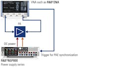
CW-based tests range from measuring the gain and impedance match over the frequency of operation to an understanding of the distortion introduced when it’s driven into nonlinear behavior, for example, compression, harmonics, and intermodulation. These tests, as well as the noise figure, efficiency, and power-added efficiency (PAE) can all be conducted using an appropriate vector network analyzer (VNA) such as the R&S ZNA together with a power supply (Fig. 1).
Measurement of compression points is used to understand the amplifier’s useful power range before it becomes significantly nonlinear and approaches saturation. Typically, power versus gain is measured using a VNA and the 1- or 3-dB compression point is determined. Evaluating the efficiency is achieved by measuring the power supply’s power consumption and comparing this with the additional RF power delivered by the output of the amplifier.
PAE evaluates the efficiency of an amplifier in terms of how effectively it adds power to an RF signal. It can be determined by using a VNA to measure input and output RF power, and a power supply to measure how much electrical power is consumed by the amplifier.
Another important indicator of nonlinearity involves the frequency components introduced by an amplifier due to intermodulation and harmonic distortion. To conduct the intermodulation test, two signals at a specific offset and power levels are fed into an amplifier and the second- and third-order intermodulation products are measured. They’re then compared with the fundamental frequency signals to calculate IM2 and IM3.
Harmonic distortion is measured by running a CW signal into the power amplifier and measuring its output at multiples of the fundamental frequency. The frequency-conversion measurement capability of the VNA can be used since the harmonics are 2X, 3X, 4X, etc., of the frequency of the original input frequency.
Also vital in understanding the linearity of the amplifier is the third-order intercept point (IP3). It’s a mathematical approximation of the comparison between the linear behavior and how fast the third-order harmonic is increasing.
Noise figure results in a reduced dynamic range, and a reduced signal-to-noise ratio (SNR) is an indication of the noise added by the amplifier itself. To measure the noise figure, the output noise versus the input noise is evaluated with the device's gain. The cold-source method employs a VNA as a source and measurement receiver; it measures noise while the source is turned off and gain while the source on.
Alternatively, the Y-factor method uses a spectrum analyzer and a noise source. Two measurements are conducted: one with the noise source turned on and one with the noise source turned off. Plotting the two results, a line is taken through the measured points to derive the noise added by the amplifier alone.
From CW to Modulated Testing
Using a VNA to conduct continuous-wave testing can provide a lot of information about the amplifier’s overall performance. However, modulation-based testing lets us see how the device will perform using the specific wireless standard it’s intended for, such as 5G or Wi-Fi. For these types of tests, we need a vector signal generator (VSG) and a spectrum analyzer with appropriate frequency coverage and bandwidth (Fig. 2).
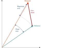
In modulation-based testing, the most important metric to characterize modulation quality is error vector magnitude (EVM). Each symbol in an I/Q constellation has an ideal or reference point that corresponds to a defined magnitude and phase, but received or measured points rarely fall exactly on the ideal point. Some of the differences are due to magnitude error and others due to phase error.
We can quantify these two sources of error by drawing a vector that connects the reference and measured points, referred to as the “error vector” (Fig. 3). The root mean square (RMS) average amplitude of the error vector, normalized to ideal signal amplitude reference, is the EVM, expressed either as a percentage or in decibels. EVM is measured at each symbol time. Larger values of EVM mean a higher probability that the receiver will mistake one symbol for another, resulting in bit errors.
Measured I/Q points can be visualized in an I/Q diagram and compared with their ideal values using a constellation diagram on a spectrum analyzer. This is a very useful tool for the amplifier designer because it gives insight into the overall modulation quality. Furthermore, how the errors are distributed is indicative of specific issues with the amplifier performance, such as phase noise, random noise, or compression.
Linearization Approaches
Amplifier linearization can be done in various ways. The most common approach is to use digital predistortion (DPD) of the signal (Fig. 4), where the incoming waveform is modified on the fly in a device implementation to compensate for the nonlinear behavior of the power amplifier. It helps to improve signal quality and reduce EVM, while minimizing the adjacent channel leakage ratio when utilizing multiples of the signal bandwidth.
DPD, which uses mathematical algorithms, can be realized in several ways. A test-instrument assisted approach to develop DPD can deliver fast results with a straightforward process flow, offering an easy way to understand an amplifier’s optimum performance with DPD. As RF PA designers, we want to understand how well we can linearize its behavior with predistortion and operate an amplifier close to compression where efficiency is highest.
The measurements required to create a model of the power amplifier can be done efficiently using the R&S SMW200A VSG with the R&S FSW signal and spectrum analyzer. The internal waveform-generation capabilities of the signal generator create various standard-compliant test signals, such as 5G. The analyzer performs all characterization measurements required for any test signal from a single data acquisition. The input signal is manipulated in an iterative process to achieve the best result for a given operating point.
The FSW analyzer allows for two DPD modes—the real-time polynomial approach, which fits the needs for mobile devices, and Direct DPD, which provides ideal predistortion, including memory effect, by correcting the signal on a sample-by-sample basis.
Efficiency Enhancements
Envelope tracking (ET) is a very common optimization technique employed in designs of battery-powered devices like mobile phones. A combination of VSG and spectrum analyzer (Fig. 5) form a simple but powerful test setup for ET applications. The ET technique avoids wasted energy being dissipated as heat and maximizes the battery life, making the device much more efficient.
The crest factor describes the ratio between the peak and the average power in the signal. Some high-power peaks are statistically extremely rare. However, to transmit the whole signal linearly, they need to be kept within the linear range of the amplifier. These high peaks can create intermodulation, but when the signal into the amplifier is modified by cutting off rare peaks, the effect on the signal content is minimal. In addition, the complete remaining signal can be shifted closer toward the maximum linear range of the device.
Integrated Test Setup
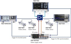
Combining the instruments of the CW and modulated signal tests to create an integrated amplifier test stand (Fig. 6) not only provides complete test coverage with the required flexibility and accuracy, but also enables synchronized measurements. Furthermore, having one connection to the DUT for all tests allows for faster and smoother testing without re-cabling.
In summary, high-throughput wireless communications systems require higher-order modulation schemes to increase the number of bits per symbol in a given bandwidth, causing the symbols to be closer together. This, in turn, requires higher modulation and demodulation accuracy to avoid bit errors.
EVM is the primary key performance indicator (KPI) of modulation quality. Deriving and analyzing EVM to understand the cause of signal imperfections is an essential tool for RF power-amplifier designers.
A combination of CW and modulation testing are applied for complete evaluation of designs during the development, validation, and production of RF power amplifiers. The process can be structured by first conducting fundamental characterization of the amplifier using CW techniques, using modulated signals for wireless standard-specific testing, and then implementing linearization in a particular DPD.
This can be achieved very efficiently with a surprisingly simple test setup consisting of a VNA, VSG, signal analyzer, and power supply. It provides the designer with a complete solution for developing amplifiers that can operate over wide bandwidths using higher-order modulation signals.
References
“Testing RF power amplifier designs,” Rohde & Schwarz GmbH & Co. KG, PD 3608.0391.92, Version 01.00, November 2023.
“RF amplifier testing -from wafer to design-in,” Rohde & Schwarz, PD 5215.7568.32, Version 02.02, April 2023.
“Understanding EVM,” Paul Dominowski, Rohde & Schwarz GmbH & Co. KG, PD 3683.8038.52, Version 01.00, October 2022.


