Advanced Nonlinear and Noise Modeling of High-Frequency GaN Devices

Download this article as a .PDF
Gallium-nitride (GaN) technology has been rapidly growing as the material of choice for HEMT devices in the RF/microwave industry due to its high-efficiency operation and its specific properties being ideal for high-frequency and high-power applications. GaN technology has also proven applicable for high-frequency, low-noise receiver circuitry. More recent processes in GaN transistor development have used shorter gate lengths to address increasing opportunities for use in designs at 10 GHz and above.
This expanding utilization of GaN technology has led to demand for highly accurate, nonlinear advanced models that are effective for electronic design of various modes of high-efficiency power amplifiers (PAs), as well as low-noise applications. This article focuses on the features and capabilities of a set of advanced models for Qorvo’s 0.15-µm GaN die devices for both nonlinear and low-noise high-frequency designs.1
Qorvo GaN15 Technology
The Qorvo GaN 15 (QGaN15) process is shorter gate length technology capable of supporting applications through 40 GHz, as compared to QGaN25 (for applications to 18 GHz) and QGaN50 (for applications to 10 GHz).2 The process uses AlGaN/GaN epitaxial layers grown on high thermal conductivity silicon-carbide (SiC) substrate. Performance parameters of the QGaN manufacturing technology include maximum currents of 1.15 A/mm and maximum frequency of oscillation (fmax) as high as 160 GHz,3 with nominal operating voltage of 28 V.
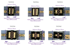
Models for six of the many transistor devices available from Qorvo are now included in the Modelithics Qorvo GaN Library.4 These are the TGF2933, TGF2934, TGF2935, TGF2936, TGF2941, and TGF2942 (Fig. 1). Two model versions were developed for each of the six discrete die transistors, a small-signal/noise model and a nonlinear model. The small-signal/noise model provides for highest linear and noise simulation accuracy in comparison with the small-signal simulations of the nonlinear models. However, for these die, the nonlinear models also provide good predictions of small-signal S-parameters and noise parameters if designers happen to prefer to use the same model for both linear and nonlinear simulations.
Small-Signal/Noise GaN HEMT Model Versions
The small-signal transistor models are optimized for broadband S-parameters and noise at specific operating bias conditions. These models offer slightly enhanced model-to-measured accuracy for the small signal simulation, which is of primary importance in low-noise amplifier (LNA)/receiver applications. In such applications, the use of a GaN device may be preferred due to tolerance to large-signal inputs (therefore eliminating the need for limiter circuitry) and/or linearity requirements.
Precision broadband measurements from two test bench configurations were used to validate the small-signal model version. A multi-bias S-parameter test bench was used that consisted of a vector network analyzer (VNA) along with bias tees, bias voltage source, RF wafer probe station, and a PC. Measurement calibration software was used that enabled efficient bias sweeps along with multi-line TRL calibration with custom microstrip standards.
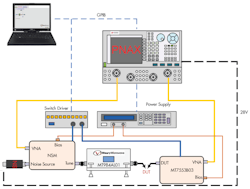
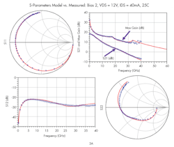
The noise parameter testing bench consisted of a Keysight PNA-X VNA, noise source, biasing equipment, Maury tuner, noise receiver module, switch box, and power distribution hub (Fig. 2). This system, which is capable of noise parameter characterization to 50 GHz, was used for noise modeling of the QGaN15 transistors to 36 GHz. Figure 3 shows the model-to-measurement accuracy of the TGF2942 small-signal model.
Large-Signal GaN HEMT Model Versions
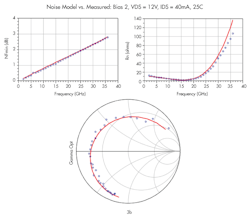
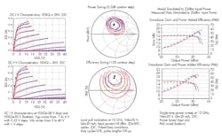
The nonlinear model versions are developed using a Modelithics-modified Angelov model implemented with Verilog-A code. They are validated with the same S-parameters and noise measurements used for the small signal model, along with current-voltage (IV) and large-signal load-pull data. The models include additional simulation features, such as scalable VDSQ range, temperature scalability, and self-heating effects. The large-signal model versions offer advanced intrinsic IV sensing for waveform optimization, making the models compatible with the latest design techniques for various classes of power amplifiers, such as Class A, AB, F, and J. Figure 4 shows example non-linear model performance data.
Summary
The use of GaN manufacturing technology is very effective and efficient for high-frequency transistor devices. The technology is advancing and the use of GaN in the RF/microwave industry is growing quickly. The availability of accurate models with advanced simulation features is very important to designers. Electronic design allows for cost-effective design optimization, but accurate models are a necessity to successful simulation.
Acknowledgements and Additional Information
This article expands upon a presentation delivered at the 2016 EDI CON conference held in September 2016 in Boston. The authors would like to thank Qorvo for collaboration related to this work as part of the Modelithics Vendor Partner (MVP) program, as well as Keysight Technologies and Maury Microwave for measurement solution collaboration.
A trial of the Modelithics Qorvo GaN Library for Keysight ADS and/or NI AWR Design Environment is available to approved designers and can be requested here.
For designer convenience, an extensive collection of documentation and example workspaces related to the Modelithics Qorvo GaN device models is available.
Larry Dunleavy, Jiang Liu, Miriam Calvo, Hugo Morales, and Laura Levesque
Raj Santhakumar
References
1. “Non-Linear and Noise Modeling of a 0.15um GaN Die Family,” presentation at EDI CON 2016.
2. “GaN: The Industry’s Hot Technology,” 2017.
3. Nayak, M-Y. Kao, H-T Chen, T. Smith, P. Goeller, W. Gao, J. Jimenez, S. Chen, C. Campbell, G. Drandova, R. Kraft, “0.15um GaN MMIC manufacturing technology for 2-50 GHz power applications,” 2015 International conference on compound semiconductor manufacturing technology, Scottsdale, Ariz.
4. Dunleavy, H. Morales, C. Suckling, and Kim Tran, “Device and PA Circuit Level Validations of a High Power GaN Model Library,” Microwave Journal, August 2016.

