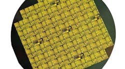
When it comes to reliability, high-performance semiconductors are largely impacted by operating temperature. Gallium-nitride (GaN) devices, which are capable of high power densities, must dissipate high amounts of heat to be effective and achieve high reliability. By using GaN-on-diamond wafers, TriQuint Semiconductor, Inc. has managed to reduce device temperature and increase thermal conductivity (see photo). According to the firm, this technology will enable new generations of RF power amplifiers (PAs) that reduce size or increase power output by a factor of three compared to today’s GaN solutions.
The firm successfully transferred a semiconductor epitaxial overlay onto a synthetic diamond substrate, preserving key GaN crystalline layers. As a result, the GaN semiconductors benefit from the high thermal conductivity of the diamond substrate and low thermal resistance at the boundary between the GaN and diamond materials. This achievement demonstrates the feasibility of GaN-on-diamond HEMT devices.
According to results attained to this point, TriQuint has achieved the goal of a three-fold improvement in heat dissipation while preserving RF functionality, which was the primary objective of the Defense Advanced Research Projects Agency’s (DARPA’s) Near Junction Thermal Transport (NJTT) program. NJTT focuses on device thermal resistance “near the junction” of the transistor. Thermal resistance inside device structures can be responsible for more than 50% of normal operational-temperature increases. In its research, TriQuint has shown that GaN RF devices can operate at a much higher power density and in smaller sizes by leveraging thermal-management techniques.
Additional fabrication improvements and extensive device testing are underway. Their goal is to optimize the epitaxial-layer transfer process and fully characterize the enhancements that can be achieved in these new HEMT devices. TriQuint demonstrated its new GaN-on-diamond, high-electron mobility transistors (HEMTs) in conjunction with partners at the University of Bristol, Group4 Labs, and Lockheed Martin under the NJTT program.
