This file type includes high resolution graphics and schematics when applicable.
Miniaturization is critical for many circuits and systems, and the use of substrate integrated waveguide (SIW) resonators has proven to support the design of compact filters. In particular, a novel triband filter based on SIW-loaded resonators provides passbands of 1.85, 2.575, and 3.05 GHz in a very small size.
The filter incorporates quarter-wavelength resonators and a loaded SIW resonant stub. The first and second passbands are obtained using the SIW-loaded resonator, which is smaller in size than a uniform impedance resonator (UIR); the quarter-wavelength resonators help generate the third passband. To demonstrate the approach and how miniaturization is possible even with three passbands, a practical filter was fabricated. The performance yielded was quite close to the predicted simulation values.
Wireless communications applications in different frequency bands have developed rapidly. In turn, this has created a rising demand for filters with dual frequency bands in support of different wireless applications, such as wireless code-division multiple-access (WCDMA) systems and wireless local area networks (WLANs). The use of dual-band filters rather than multiple separate filters in multiband communication systems can help reduce their volume and mass. As a result, many different approaches have been studied for the design of multiple-band filters.1-10
Several synthesis methods for creating multiband filters using frequency transformations have been detailed previously.1-5 Synthesis of microwave filters involves controlling the passbands analytically. Several dual-mode, dual-band bandpass filters (BPFs) have been realized by using two nested dual-mode resonators of different sizes6-8 or by means of multilayer circuit structures.9,10 But most of these multiband filters have been designed without the guidance of a straightforward synthesis method, so the design procedure isn’t exact or consistent.
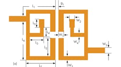
To save space even beyond what is possible with a dual-band filter, a novel triband microstrip version was developed with passbands for three different wireless communications systems. The path to the triband filter design begins with a dual-band filter with 0-deg. feed (Fig. 1), which is composed by two SIW-loaded resonators. The first and second passbands can be generated by the SIW-loaded resonators. The two passband can be adjusted to their desired values by changing the dimensions of the SIW-loaded resonators.
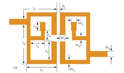
To create the third passband—and the triband filter—the quarter-wavelength resonators are embedded inside the microstrip printed-circuit board (PCB). This is done in such a way that the center frequency of the third passband can also be controlled and adjusted. To demonstrate the design approach, a triband filter with passbands of 1.69 to 2.02 GHz, 2.52 to 2.65 GHz, and 3.06 to 3.2 GHz was fabricated and measured, with the measured results showing good agreement with computer simulations.
In following this design approach, the initial dual-band filter design with SIW-loaded resonator is shown in Fig. 1(a); the filter includes two SIW-loaded resonators to produce the first and second passbands of the triband filter. Two ports with characteristic impedance of 50 Ω are symmetrical by the center of filter, and introduce transmission zeros outside of the passbands.
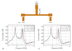
The configuration of these SIW-loaded resonators is shown in Fig. 2(a). It consists of a SIW structure and another SIW resonant stub loaded at the transmission-line center. To obtain a desired passband, the first center frequency (f1) can be controlled by tuning the length of the SIW, while the second center frequency (f2) is adjusted by tuning the length of the loaded SIW stub.
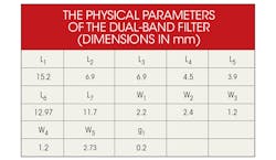
The physical parameters of the initial dual-band filter are given in the table. The relative dielectric constant of the PCB substrate material is 2.65 and the thickness of the substrate is 1 mm. Because the SIW resonant stub is loaded at the SIW center where the voltage is zero at f1, the first center frequency will not be affected by adding the SIW stub, which can be studied by even-odd-mode analysis,11 as shown in Fig. 2(a). Overall, the size of the resonator loaded with a SIW stub is smaller than other approaches, with more parameters that can be adjusted to control the frequency response.
The stub dimensions L and W can be adjusted to control the second filter passband center frequency, f2, without impacting the first filter passband center frequency, f1. Figures 2(a), (b), and (c) show simulated results for the proposed resonators with different dimensions L and W, while the other dimensions are fixed. As these results indicate, the first passband center frequency (f1) is unchanged while the second passband center frequency (f2) can be adjusted by varying the dimensions L and W.
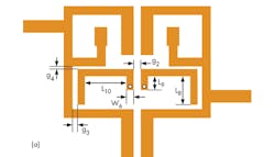
To obtain the third passband center frequency (f3), a pair of quarter-wavelength resonators are embedded in the dual-band filter [Fig. 3(a)]. The third passband frequency (f3) is mainly determined by the length of the quarter-wavelength resonators.
This file type includes high resolution graphics and schematics when applicable.
Downsizing with SiW
This file type includes high resolution graphics and schematics when applicable.
Compared with a conventional triband filter, this novel triband filter can be fabricated in a smaller footprint through its use of SIW technology. It consists of two sets of resonators: the SIW-loaded resonators and the quarter-wavelength resonators that are embedded within the PCB design. To achieve the desired bandwidths for all three passbands, separate tuning of the passbands is required.
For example, the quality factor, Qe, depends on the position of the filter tap. The coupling coefficients at center frequencies f1 and f2 are determined by coupling length L2 and coupling spacing g1. The coupling coefficients of the third filter passband are determined by length L9 and gap g3 between the quarter-wavelength resonators.
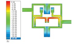
The structure of the proposed triband filter is effective in controlling the coupling of the three filter passbands between the two resonators. Figure 3 shows the current distribution of the proposed triband filter at the third resonance frequency. The current is mainly distributed at the two quarter-wavelength resonators at the third resonance frequency, in agreement with the computer simulations.
The table lists the physical parameters for the triband filter, while the other dimensions are the same as for the dual-band filter shown in Fig. 1(a). The relative dielectric constant and the thickness of the PCB substrate are 2.65 and 1 mm, respectively. The full-wave electromagnetic (EM) simulator IE3D from Mentor Graphics was used in the computer simulation of the dual-band and triband filter circuits and to extract the parameters listed in the table.
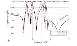
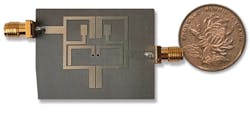
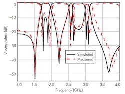
To demonstrate this design approach using SIW circuitry and a combination of resonators, a filter was fabricated (Fig. 4) and measured with a commercial vector network analyzer (VNA), a model 8719ES from Agilent Technologies (now Keysight Technologies). The measured results were compared with simulations of the design (Fig. 5) using the IE3D simulation software. According to the simulations, the triband filter produced passbands at 1.69 to 2.02 GHz, 2.52 to 2.65 GHz, and 3.06 to 3.20 GHz.
Simulations showed passband insertion losses of about 0.6 dB at the center of each band. According to the measurements, the triband filter produced passbad center frequencies at passbands at 1.85, 2.85, and 3.13 GHz, with measured insertion losses of 0.73, 1.20, and 1.30 dB, respectively, at the center of each passband. The transmission zeros out of the passband improved the frequency selectivity greatly.
In summary, a compact triband bandpass filter was presented and demonstrated, realized by means of SIW-loaded resonators working with additional quarter-wave resonators to achieve the three separate passbands. The first and second passbands are obtained by the SIW resonator, while the third passband results from the quarter-wave resonant structure. The design permits control of the center frequencies and bandwidths of the three passbands. A prototype fabricated according to this design strategy provided measured performance quite close to the simulated values.
Acknowledgments
This work was supported by the National Natural Science Foundation of China (NSFC) under project Nos. 61331005, 61001039, 61471292, and 61471292, and the 55th China Postdoctoral Science Foundation.
Jian-zhong Chen, Engineer
Jie Shen, Engineer
Ni Gao, Engineer
An-xue Zhang, Engineer
School of Electronic and Information Engineering, Xi’an Jiaotong University, Xi’an, Shaanxi, People’s Republic of China, 710049
References
1. G. Macchiarella and S. Tamiazzo, “Design techniques for dual-passband filters,” IEEE Transactions on Microwave. Theory & Techniques, Vol. 53, No. 11, November 2005, pp. 3265-3271.
2. J. Chen, J. Z. Chen, S. Fu, and C.H. Liang, “Analytical Design of Novel Dual-Band Cross-Coupled Substrate Integrated Waveguide Filter,” Microwave and Optical Technology Letters., Vol. 54, 2012, pp. 1609-1612.
3. J. Chen, J.Z. Chen, B. Wu, Y.-L. Zhang, and C.-H. Liang, “Design of Triple-Band Microstrip Filter with Transmission Zeros Using Open Stubs,” Journal of Electromagnetic Waves and Applications, Vol. 26, 2012, pp. 525-524.
4. M. Mokhtaari, J. Bornemann, K. Rambabu, and S. Amari, “Coupling matrix design of dual and triple passband filters,” IEEE Transactions on Microwave. Theory & Techniques, Vol. 54, No. 11, November 2006, pp. 3940-3946.
5. J. Lee and K. Sarabandi, “A synthesis method for dual-passband microwave filters,” IEEE Transactions on Microwave Theory & Techniques, Vol. 55, No. 6, June 2007, pp. 1163-1170.
6. H.M. Hizan, I.C. Hunter, and A.I. Abunjaileh, “Integrated dual-band radiating bandpass filter using dual-mode circular cavities,” IEEE Microwave & Wireless Component Letters, Vol. 21, No. 5, May 2011, pp. 246-248.
7. S.W. Fok, P. Cheong, K.W. Tam, and R.P. Martins, “A novel microstrip square loop dual-mode bandpass filter with simultaneous size reduction and spurious response suppression,” IEEE Transactions on Microwave Theory & Techniques, Vol. 54, No. 5, May 2006, pp. 2033-2041.
8. P. Cheong, T.S. Lv, W.W. Choi, and K.W. Tam, “A compact microstrip square-loop dual-mode balun-bandpass filter with simultaneous spurious response suppression and differential performance improvement,” IEEE Microwave & Wireless Component Letters, Vol. 21, No. 2, February 2011, pp. 77-79.
9. L. Zhu, B.C. Tan, and S.J. Quek, “Miniaturized dual-mode bandpass filter using inductively loaded cross-slotted patch resonator,” IEEE Microwave & Wireless Component Letters, Vol. 15, No. 1, January 2005, pp. 22-24.
This file type includes high resolution graphics and schematics when applicable.
