This file type includes high resolution graphics and schematics when applicable.
Substrate-integrated-waveguide (SIW) technology can bring some of the performance benefits of waveguide transmission lines to compact microstrip printed-circuit-board (PCB) components, including filters. To demonstrate some of the promise of SIW technology, a bandpass filter was designed for use at S-band frequencies. By using resonant cavities based on SIW technology, excellent filtering results were achieved in the desired frequency bands. The filter achieved a passband of 2.75 to 3.40 GHz with low passband loss, with close agreement between measured and simulated results.
Expansion of telecommunications systems in recent years has required the development of high-performance equipment at reasonable prices. This need has impacted systems at all frequencies, including at RF and microwave frequencies. Some low-loss components, such as waveguide filters, have provided good performance—albeit with a tradeoff in size and weight, where some applications were in need of lighter, more compact components. SIW technology is one of the approaches that has provided high-performance component solutions at a fraction of the size and weight of traditional rectangular waveguide components.1-4
SIW technology combines some of the performance benefits of traditional rectangular waveguide with the compact size of planar transmission lines. The waveguide benefits include low loss, compact size, high quality factor (Q), and the potential for handling high power levels with low electromagnetic (EM) radiation. SIW approaches allow different components to be designed and constructed as integrated components using a single manufacturing process, rather than building them separately and then combining them into a subassembly.
Filters, phase shifters, antennas, and other components can be designed and constructed in SIW rather than in rectangular waveguide. This helps to reduce both the overall dimensions of a telecommunications system and the cost of manufacturing these components. Although SIW technology is still relatively new and not considered a mature technology, it has been applied to a number of different components and subsystems by different design teams and has shown consistent, stable performance over time and temperature.
In addition, with time, a growing number of SIW component models become available in commercial computer-aided-engineering (CAE) circuit simulation software. As examples, filters, couplers, and slot antennas have already been made with this technology with good results.5-13 In addition, a number of different methods have been used for the characterization of these components to better understand the performance and behavior of SIW components.14-19
Filters, of course, are one type of component widely used in modern telecommunications systems, both for processing and providing selectivity among different signals. To explore the capabilities of SIW technology for fabricating filters for communications applications, a bandpass filter was designed for S-band frequency use based on SIW technology. A commercial circuit simulation software program, CST Microwave Studio from Computer Simulation Technology,20 was used to simulate the performance of the SIW bandpass filter design and help determine the validity of the design approach.
The cutoff frequency, fc, for the transverse-electromagnetic (TE) mode of an SIW component is the same of that for a waveguide filled with a dielectric material having relative permittivity of εr, as computed by Eq. 1:
fc = v/2π[(mπ/a)2 + (nπ/b)2]0.5 (1)
where:
m and n = mode numbers,
b = waveguide dimensions, and
v = c/(εr)0.5 (2)
and
v = the relative velocity through the dielectric-filled waveguide,
c = the speed of light, and
εr = the relative permittivity of the dielectric material.
For operation in the transverse-electromagnetic TE10 mode, Eq. 1 can be simplified to the form of Eq. 3:
fc = v/2a (3)
where dimension a equals the width of a rectangular waveguide filled with dielectric material of relative permittivity, εr, and can be found by means of Eq. 41,2:
a = c/2fc(ε)0.5 (4)
where:
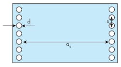
aSIW = a + d2/0.95p (5)
and
d = the diameter of the viaholes, and
p = the distance between the viaholes.
When designing SIW circuits, a number of conditions are required, including those detailed by Eqs. 6 and 7:
d < λg/5 (6)
p To adapt a microstrip feedline to an SIW guide, it is necessary to calculate the impedance of the SIW guide according to Eq. 8: Zpi = ZTE(π2h/8as) (8) where ZTE represents the wave impedance for the TE10 mode, as given by Eq. 91,2: ZTE = (μ/ε)0.5 (9)
This file type includes high resolution graphics and schematics when applicable.
A Closer Look
This file type includes high resolution graphics and schematics when applicable.
For the design of an SIW filter operating at S-band frequencies (2 to 4 GHz), the design equations were used to calculate the SIW dimensions. For operation on the TE10 mode, the cutoff frequency, fc, of 2 GHz was calculated from the effective width of the guide for a dielectric material with relative permittivity, εr, of 2.17 when measured through the z direction (thickness) of the material at 10 GHz and dissipation factor of 0.0013 at 10 GHz. The nonwoven, fiberglass-reinforced polytetrafluoroethylene (PTFE) dielectric material is known commercially as IsoClad 917, and is available from Arlon Materials for Electronics.
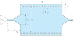
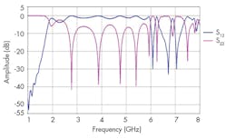
After calculating the input impedance of the SIW filter, the next step involved the design of a taper transition for the filter. Figure 2 shows a top view of the SIW waveguide with two tapers operating in the S-band range. Figure 3 presents the performance of this SIW guide with SIW transitions in terms of transmission and reflection. Below the design cutoff frequency, fc, of 2 GHz, minimum transmission and maximum reflection can be seen in Fig. 3.
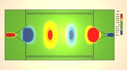
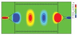
Beyond 2 GHz, the transmission characteristics improve significantly by means of the taper transition. Several resonant peaks show levels to -41 dB. Figure 4 presents the magnetic-field propagation within the SIW structure at 3 GHz.
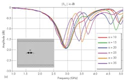
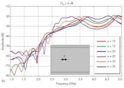
For the design of the filter’s resonant cavities, it was necessary to add several metal viaholes to the SIW structure. As part of the design process, two viaholes were inserted and the impact of varying distance a between the viaholes was analyzed. Figure 5 offers return losses and transmission coefficients for different values of parameter a for the SIW filter.
According to Fig. 5, good bandpass filter characteristics were achieved for a distance of 35 mm. As the distance between the viaholes increased, the filter passband and the cutoff frequency moved higher in frequency. To design a practical transition for the SIW filter input, a taper was optimized and integrated into the SIW filter.
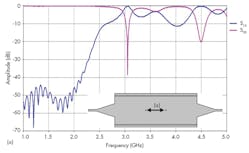
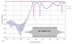
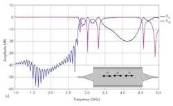
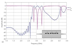
Figure 6 shows the topology of the SIW filter and its transmission and reflection performance from 1 to 5 GHz. Unfortunately, the design exhibits poor rejection in the band from 1 to 5 GHz. To improve rejection, it is necessary to increase the number of cavities in the SIW filter design. Figures 6(b), (c), and 6(d) show the results of filter topologies with two and three cavities; the performance of the design with the SIW transition, in terms of transmission and reflection, is plotted in those same figures.
Good rejection was achieved when three cavities were used, although adapting the design to an increased number of cavities required some modifications. To improve the design for use with three cavities, it was thought that the dimensions of the tapers could be adjusted appropriately. Figure 6(d) shows an optimized filter topology after several changes.
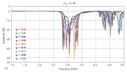
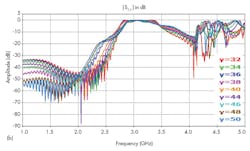
The position of the viaholes in the cavities was another structural design parameter that was analyzed for its impact on the SIW filter’s performance. The performance of the SIW structure was studied for different positions of the viaholes within the resonant cavities. Figure 7 shows the filter with its modified cavities, and Fig. 8 offer some of the results of this study. Responses are plotted for return loss and transmission coefficient for different positions of the viaholes. From this analysis, it was found that optimum matching conditions occurred at y = 10 mm.
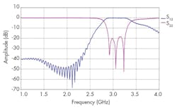
Figures 9 and 10 show the final topology of the filter and the responses for that construction, respectively. In particular, Fig. 10 offers curves for the return-loss and transmission coefficient performance projections from 1 to 5 GHz. A filter bandwidth from 2.75 to 3.40 GHz beyond the S-band passband was recorded, with good impedance matching and acceptable levels of rejection beyond the filter passband.
The filter was fully simulated with commercial simulation software—CST Microwave Studio from Computer Simulation Technology. It offers great promise for communications applications at S-band and higher (with reduced dimensions).
Boualem Mansouri, Doctor
Mehadji Abri, Doctor
Telecommunications Laboratory, Faculty of Technology, University of Tlemcen, Algeria
Hadjira Abri, Doctor
STIC Laboratory, Faculty of Technology, University of Tlemcen, Algeria
Mohamed Amine Rabah, Doctor
Telecommunications Laboratory, Faculty of Technology, University of Tlemcen, Algeria
Junwa Tao, Professor
Tan-Hoa Vuong, Doctor
LaPlace Laboratory, Ensheeiht, University of Toulouse, France
This file type includes high resolution graphics and schematics when applicable.
References
This file type includes high resolution graphics and schematics when applicable.
1. M.A. Rabah, M. Abri, J. Tao, and T.H. Vuong, “Substrate integrated waveguide design using the two dimentionnal finite element method,” Progress In Electromagnetics Research M, Vol. 35, 2014, pp. 21-30.
2. S. Doucha, and M. Abri, “New design of leaky wave antenna based on siw technology for beam steering,” International Journal of Computer Networks & Communications, Vol. 5, No. 5, September 2013.
3. Yong Ju Ban, “Tunable Ferrite Phase Shifters Using Substrate Integrated Waveguide Technique,” Ph.D. thesis, December 2010.
4. K. Wu, D. Deslandes, and Y. Cassivi, “The substrate integrated circuits—A new concept for high frequency Electronics and Optoeletronics,” Microwave Review, No. 12, December 2003, pp. 2 -9.
5. Xiao-Ping Chen, Ke Wu, and Zhao-Long Li,, “Dual-Band and Triple-Band Substrate Integrated Waveguide Filters With Chebyshev and Quasi-Elliptic Responses,” IEEE Transactions on Microwave Theory & Techniques, Vol. 55, December 2007, pp. 2569-2577.
6. Y. Cassivi, L. Perregrini, P. Arcioni, M. Bressan, K. Wu, and G. Conciauro, “Dispersion characteristics of substrate integrated rectangular waveguide,” in IEEE Microwave & Wireless Component Letters, Vol. 12, September 2002, pp. 333-335.
7. Y. Cassivi and K. Wu, “Low cost microwave oscillator using substrate integrated waveguide cavity,” IEEE Microwave & Wireless Component Letters, Vol. 13, No. 2, February 2003, pp. 48-50.
8. J.A. Ruiz-Cruz, M.A.E. Sabbagh, K.A. Zaki, J.M. Rebollar, and Y. Zhang, “Canonical ridge waveguide filters in LTCC or metallic resonators,” IEEE Transactions on Microwave Theory & Techniques, Vol. 53, No. 1, January 2005, pp.174-182.
9. W. Hong, B. Liu, Y.Q. Wang, Q.H. Lai, and K. Wu, “Half mode substrate integrated waveguide: A new guided wave structure for microwave and millimeter wave application,” in Proceedings of the Joint 31st International Infrared Millimeter Wave Conference/14th International Terahertz Electronics Conference, Shanghai, China, September 2006, pp. 18-22.
10. B. Liu, W. Hong, Y.Q. Wang, Q.H. Lai, and K. Wu, “Half mode substrate integrated waveguide (HMSIW) 3 dB coupler,” IEEE Microwave & Wireless Components Letters, Vol. 17, No. 1, January 2007, pp. 22-24.
11. Y. Wang, W. Hong, Y.D. Dong, and B. Liu, “Half mode substrate integrated waveguide (HMSIW) bandpass filter,” IEEE Microwave & Wireless Component Letters, Vol. 17, No. 4, April 2007, pp. 2560-267.
12. B. Liu, W. Hong, Y. Zhang, H.J. Tang, X.X. Yin, and K. Wu, “Half mode substrate integrated waveguide 180 3-dB directional couplers,” IEEE Transactions on Microwave Theory & Techniques, Vol. 55, No. 12, December 2007, pp. 2586–2592.
13. Y. Cheng, W. Hong, and K.Wu, “Half mode substrate integrated waveguide (HMSIW) directional filter,” IEEE Microwave & Wireless Component Letters, Vol. 17, No. 7, July 2007, pp. 504–506.
14. J.E. Rayas-Sanchez and V. Gutierrez-Ayala, “A General EM-Based Design Procedure for Single-Layer Substrate Integrated Waveguide Interconnects with Microstrip Transitions,” IEEE MTT-S International Microwave Symposium Digest, Atlanta, GA, June 2008, pp. 983-986.
15. V.N. Kanellopoulos and J.P. Webb, “A Complete E-Plane Analysis of Waveguide Junctions Using the Finite Element Method,” IEEE Transactions on Microwave Theory and Techniques, Vol. 38, 1990, pp. 290-295.
16. R. Coccioli, R.R. Pelosi, R. Coccioli, and S. Selleri, “Optimization of Bends in Rectangular Waveguide by a Finite Element-Genetic Algorithm Procedure,” Microwave and Optical Technology Letters, Vol. 16, No. 5, December 1997, pp. 287-290.
17. D.-K. Sun, L. Vardapetyan, and Z. Cendes, “Dimensional Curl-Conforming Singular Elements for FEM Solutions of Dielectric Waveguide Structures,” IEEE Transactions on Microwave Theory and Techniques, Vol. 53, No. 3, March 2005, pp. 984-992.
18. A. Zeid and H. Baudrand, “Electromagnetic scattering by metallic holes and its applications in microwave circuit design,” IEEE Transactions on Microwave Theory & Techniques, Vol. 50, No. 4, April 2002, pp. 1198-1206.
19. G. Fedi, S. Manetti, G. Pelosi, and S. Selleri, “FEM-Trained Artificial Neural Networks for the Analysis and Design of Cylindrical Posts in a Rectangular Waveguide,” Electromagnetics, Vol. 22, 2002, pp. 323-330.
20. Computer Simulation Technology, El Segundo, CA.
This file type includes high resolution graphics and schematics when applicable.
