This file type includes high-resolution graphics and schematics when applicable.
Wideband communications technology is no longer a luxury—it’s become a necessity. Because communications has moved beyond voice to include video and massive amounts of data on a regular basis, wireless communications technologies have evolved from “primitive” first-generation analog cellular networks and telephones to the current third-generation (3G) and fourth-generation (4G) systems and beyond. Now these technologies are homing in on wideband fifth-generation (5G) wireless networks and a plethora of supported wireless devices.
Of course, wideband transmitters and receivers are needed to support such networks, with performance levels that can literally cut through the noise of earlier systems. As integrated-circuit (IC) technology would have it, one solution lies in having multiple wideband transmitters and receivers on a single chip, the highly integrated RadioVerse AD9371 transceiver from Analog Devices. Packed with performance, this impressive device provides a frequency range from 300 MHz to 6 GHz and wide bandwidths of 100 MHz to enable the next generation of wireless communications.
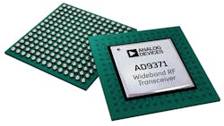
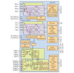
The model AD9371 direct-conversion transceiver IC (Fig. 1) integrates almost all of the components needed for a high-performance radio solution, with two independent transmitter paths and two independent receiver paths (Fig. 2). The differential transmitters and receivers are programmable and support frequency-division-duplex (FDD) and time-division-duplex (TDD) operation in 3G, 4G, and one day, 5G wireless systems.
In addition, the AD9371 includes a two-input observation receiver and a three-input sniffer receiver. The observation receiver operates much like the main receivers, with two differential inputs. The inputs share a common RF front-end ADC and baseband circuitry, so that only one observation receiver can be active at one time. The observation receiver is useful for observing the power-amplifier (PA) output for systems implementing digital predistortion techniques to improve PA efficiency.
The sniffer receiver provides three differential input ports that can be used to monitor three different frequency bands. Each input is connected to an LNA that feeds a single mixer. The maximum channel bandwidth of the sniffer receiver is 20 MHz. All of the receivers tune across a 300- to 6000-MHz frequency range.
The IC doesn’t require an external local oscillator (LO), since it contains multiple voltage-controlled oscillators (VCOs), loop filters, and three fractional-N phase-locked loops (PLLs). It does require a stable, external low-phase-noise differential clock operating between 10 and 320 MHz to generate the RF LO signals and all internal converters, digital clocks, and interface clocks. It also requires at least one external bypass capacitor, but very little else.
This is not just an analog transceiver, however. It includes multiple analog-to-digital converters (ADCs) and digital-to-analog converters (DACs) in support of the analog receiver and transmitter circuits, respectively. The IC provides self-calibration for dc offset, wideband dynamic quadrature error correction (QEC), transmit LO leakage, and digital-signal-processing functions like programmable FIR, decimation, and interpolation filters. The IC is backed by comprehensive software support and robust algorithms to ensure outstanding linearity across the wide bandwidths and the AD9371’s total frequency range.
The transceiver uses simple-to-use API or Linux drivers to communicate with a baseband processor via an SPI port. It supports JESD204B digital data serial interface for transferring data at 6 Gb/s and, in spite of the massive functionality of its multiple transmitters, receivers, and digital hardware, consumes only about 5 W power. That breaks down to about 2 W for the two receivers, 2 W for the transmitters, and about 0.8 W for the observation receiver.
Of course, commercial communications is just one possible application area for this device. With its bandwidth and flexibility, it is a candidate for military manpack and vehicular tactical radios, in signal-intelligence (SIGINT) and electronic-warfare (EW) systems, and for a host of different test instruments, such as network and spectrum analyzers.
Tracing the Evolution
The two-receiver, two-transmitter concept is not new. The AD9371 is actually an evolution of the firm’s earlier model AD9361 transceiver IC (see Microwaves & RF, May 2016, p. 45). The new chip has a much higher level of integration and a serious upgrade in performance in an attempt to eliminate external components, simplify the radio system, and ultimately deliver lower cost, size, power, and development-time benefits.
Both transceivers employ direct-conversion architectures, also known as homodyne radios. In this approach, input RF signals to the receiver are mixed with LO signals at the same frequency to produce a signal at baseband or dc, also known as a zero-IF receiver. By translating input signals so low in frequency, filtering is simplified (by means of lowpass filters in the AD9371) and the baseband signals can then be efficiently converted by on-chip ADCs (Fig. 2, again).
The many challenges with classic direct-conversion approaches, such as LO leakage and I/Q imbalance, have been overcome in the AD9371 through careful design and circuit layout, in addition to leveraging breakthrough error-correction algorithms. Furthermore, very close attention was paid to the placement of the RF ports, chip layout, and laminate design to achieve isolation between the two transmitters, and between either transmitter or either receiver, of better than 60 dB when tested with LOs at 2.6 and 3.5 GHz.
Probing the Performance
Taking a closer look at the AD9371’s various sections, the two transmitters operate with signal bandwidths as wide as 100 MHz over a total bandwidth of 300 to 6000 MHz. They are supported by a transmit synthesis bandwidth of 250 MHz and amplitude flatness of ±0.5 dB across that bandwidth when compensated by a programmable finite-impulse-response (FIR) filter. For any 20-MHz bandwidth, the amplitude flatness can be improved to ±0.15 dB with the same programmable FIR filter. The deviation from linear phase is 10 deg. across the transmit synthesis full 250-MHz bandwidth.
The transmitters deliver a maximum output of +7 dBm at 2.6-GHz LO and as much as +6 dBm for a 3.5-GHz LO. Transmit power can be controlled over a range of 0 to 42 dB with 0.05-dB resolution. The two transmitters are well isolated, with 65 dB or more isolation between transmitters when measured for LOs at 2.6 and 3.5 GHz. When tested using four UMTS carriers, the adjacent-channel leakage ratio (ACLR) is –64 dBc for a 2.6-GHz LO and –63 dBc for a 3.5-GHz LO. The in-band transmitter noise is –155 dB full scale (FS)/Hz. Image rejection is 65 dB for either of the two LOs, while carrier leakage measures –81 dBFS for either LO. The third-order output intermodulation intercept point (IIP3) is +27 dBm for the 2.6-GHz LO and +25 dBm for the 3.5-GHz LO.
The two main receivers operate at center frequencies from 300 to 6000 MHz with tunable instantaneous signal bandwidths from 5 to 100 MHz. They include a gain adjustment range of 0 to 30 dB, which can be set in 0.5-dB steps. The maximum recommended input power is –14 dBm. The amplitude ripple for any 100-MHz bandwidth is ±0.5 dB, which reduces to ±0.2 dB for any 20-MHz bandwidth. Receive and image rejection is 75 dB or better.
As with the transmitters, the receivers were characterized with LOs of 2.6 and 3.5 GHz, and were found to have noise figures of 14 and 15 dB, respectively, when operating with those two LOs. The IIP3 is –22 dBm for the lower-frequency LO. The second-order input intermodulation intercept point (IIP2) is –65 dBm for either LO.
As noted earlier, one of the chief challenges in highly integrated RF designs involves achieving good port-to-port isolation, but the separate function blocks of the AD9371 are well isolated. The isolation between receiver 1 and transmitter 1 and receiver 2 and transmitter 2 is 68 dB for the 2.6-GHz LO and 62 dB for the 3.5-GHz LO. The isolation between receiver 2 and transmitter 1 and receiver 1 and transmitter 2 is 70 dB for the 2.6-GHz LO and 62 dB for the 3.5-GHz LO. The isolation between the receivers themselves is 60 dB. The LO leakage is well controlled, with receiver LO leakage of -65 dBm for the 2.6-GHz LO and -62 dBm for the 3.5-GHz LO, both at maximum input gain. The in-band spurious content referenced to the RF input is –95 dBm, also at maximum gain.
Performance levels of the observation and sniffer receivers are similar. They cover the same total bandwidth, with 250-MHz bandwidth for the observation receiver and 20-MHz bandwidth for the sniffer receiver.
The AD9371 transceiver IC is an evolution of the company’s highly regarded AD9361 transceiver, but in many ways, it also represents a revolution for wideband radio designers. It is a single chip, supplied in a 196-ball ball-grid-array (BGA) chip-scale package (CSP) measuring 12 × 12 mm, that can handle all of the radio functions over a bandwidth wide enough to serve many of today’s wireless applications in the commercial, industrial, and military sectors. If ever there was a case of “one chip fits all,” it is the RadioVerse AD9371 transceiver IC.
Analog Devices Inc., One Technology Way, P. O. Box 9106, Norwood, MA 02062-9106; (781) 329-4700, www.analog.com.
Looking for parts? Go to SourceESB.


